Nitride semiconductor laser device and method of producing the same

a technology of nitride and laser device, which is applied in the direction of semiconductor laser, laser details, nanooptics, etc., can solve the problem of determining all chips (b) as defectiv

Active Publication Date: 2007-09-20
SHARP FUKUYAMA LASER CO LTD
View PDF2 Cites 237 Cited by
  • Summary
  • Abstract
  • Description
  • Claims
  • Application Information

AI Technical Summary

Benefits of technology

[0020]The present invention has been made to solve the aforementioned problems, and makes it possible that, when nitride semiconductor laser devices of a small width are handled in an automatic chip inspection apparatus or an automatic mounting apparatus, only some particular chips can be selected readily and automatically by image recognition.

Problems solved by technology

However, when a nitride semiconductor laser device has a reduced width, problems arise in a laser device fabricated by a technique described below.
The laser bar in such a state as above may cause problems as described below during the subsequent process of producing laser devices.
In the case of using an automatic chip inspection apparatus, if the apparatus is set to determine the position of the ridge-like stripe in chip (A) as normal, then there is a problem that it determines all of chips (B) as defective.

Method used


Image

  • Nitride semiconductor laser device and method of producing the same
  • Nitride semiconductor laser device and method of producing the same
  • Nitride semiconductor laser device and method of producing the same

Examples


first embodiment

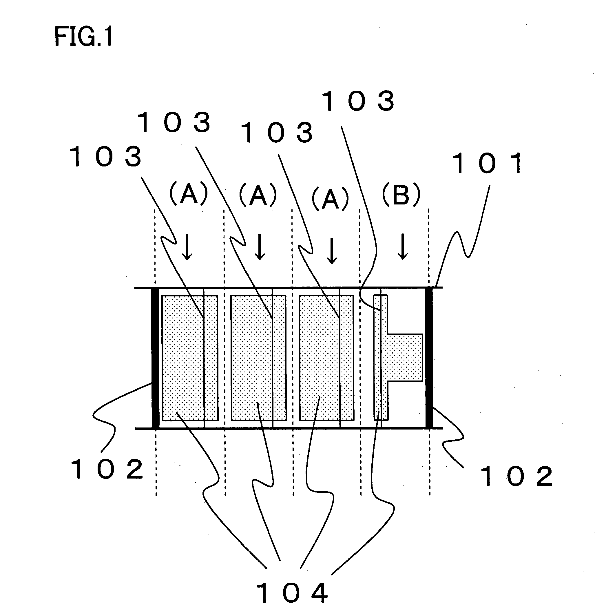
[0049]FIG. 1 is a schematic plan view showing nitride semiconductor laser devices in a state of a laser bar according to a first embodiment of the present invention. In a laser bar 101 of this drawing, there are formed a plurality of trenched regions 102. Between trenched regions 102, a plurality of ridge-like stripes 103 are formed, and a plurality of p-side electrode pads 104 are formed to cover ridge-like stripes 103. Every dotted line in FIG. 1 indicates a chip division plane.

[0050]In the first embodiment, an area ratio of p-side electrode pad 104 to the upper surface area (hereinafter referred to as a chip area) of a nitride semiconductor laser device (B) is less than 90% differently from that of a nitride semiconductor laser device (A).

[0051]In an automatic chip inspection apparatus that uses an automatic image recognition process, it is preset to determine whether a chip is acceptable or not based on the shape of p-side electrode pad 104 and preset to determine nitride semico...

second embodiment

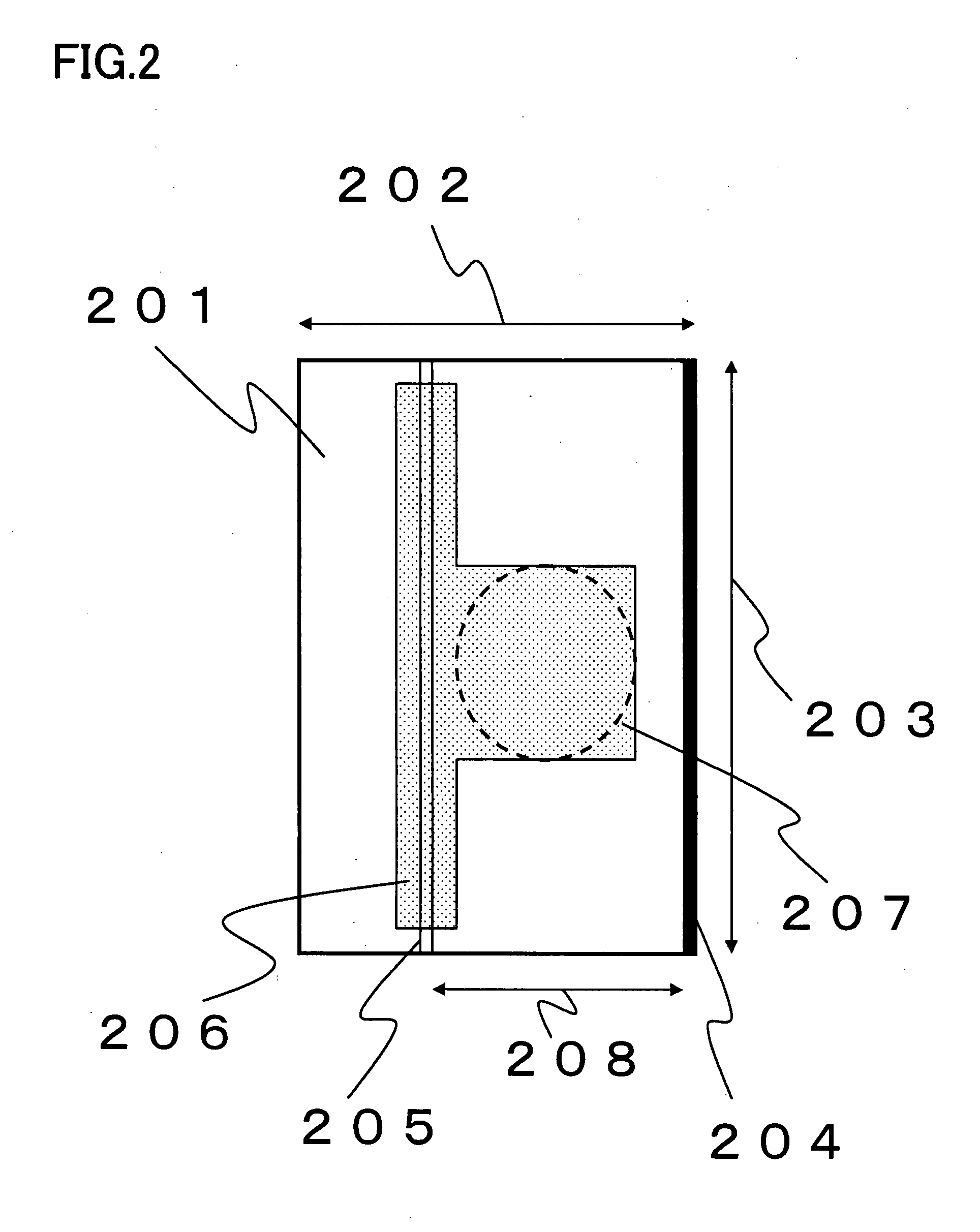
[0069]FIG. 5 is a schematic plan view illustrating a shape of a p-side electrode pad of a chip (B) as a nitride semiconductor laser device according to a second embodiment of the present invention. In this drawing, a nitride semiconductor laser device 501 is set to have a width 502 of 50 to 250 μm (e.g., 200 μm) and a length (corresponding to a resonator length) 503 of 300 to 1500 μm (e.g., 600 μm). A trenched region 504 of a worked substrate exists along the right side of chip 501. A ridge-like stripe 505 is formed at a position spaced by a distance 508 of 120 μm from the right side of the chip. A p-side electrode pad 506 is formed to include its partial area placed to cover ridge-like stripe 505 and another partial area (e.g., a square with a side of 80 μm) including a circle 507 of 80 μm diameter for wire bonding. P-side electrode pad 506 is formed with its area falling in a range of more than 2% and less than 90% of the chip area.

[0070]Circular area 507 for wire bonding is place...

third embodiment

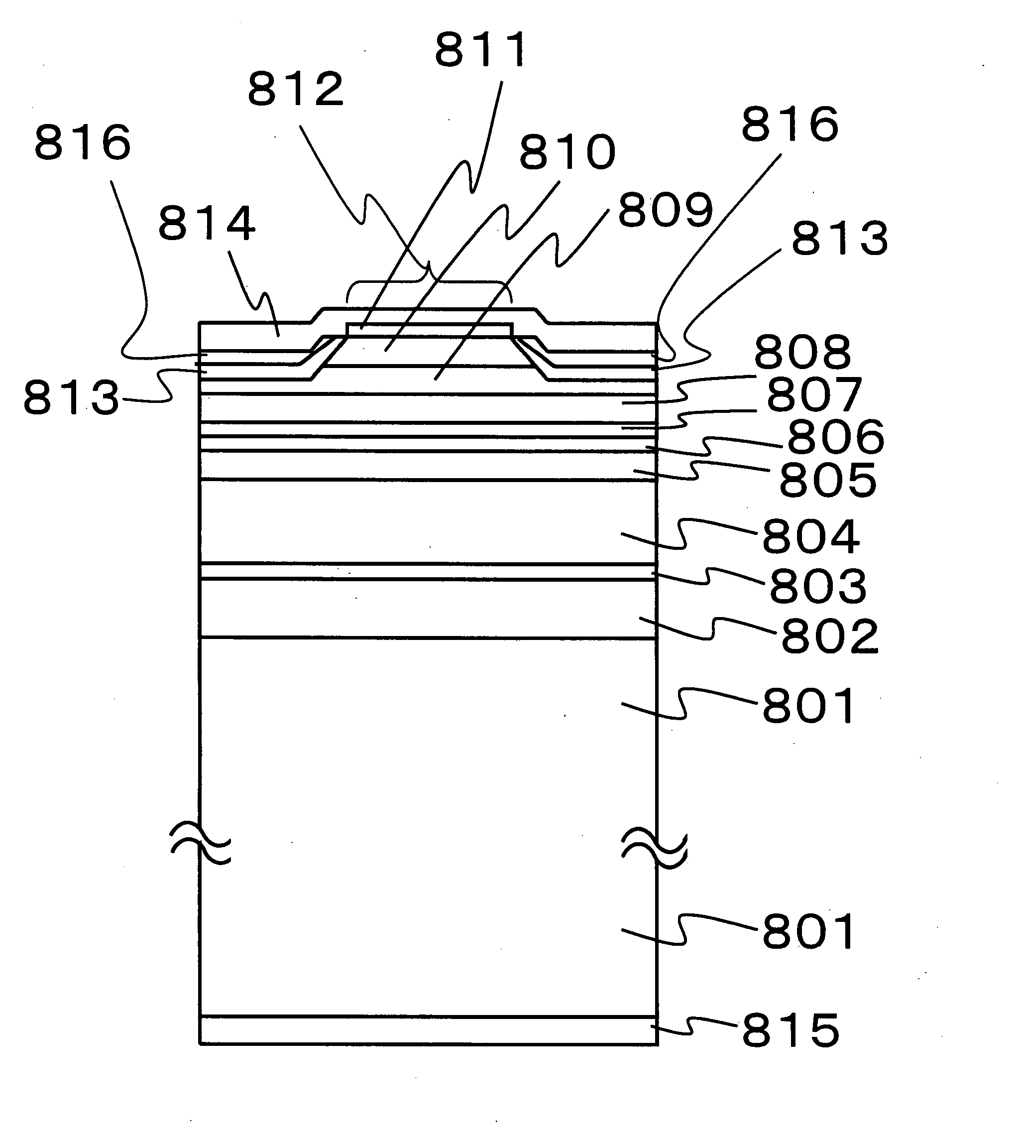
[0072]FIG. 6 is a schematic cross-sectional view showing a main part of a layered structure in a nitride semiconductor laser device according to a third embodiment of the present invention. The cross-sectional structure of FIG. 6 is different from that of FIG. 8 only in that metal layer 816 of less than 0.1 μm thickness is replaced by a layer 616 of a light absorbing material of more than 10 nm thickness. That is, other layers 601 to 615 in FIG. 6 correspond to layers 801 to 815 in FIG. 8, respectively. Further, the p-side electrode pad in the nitride semiconductor laser device of the third embodiment can have a shape identical to that of the first or second embodiment.

[0073]Since light absorbing layer 616 is formed on insulating film 613 in the nitride semiconductor laser device of the third embodiment, an area having p-side electrode pad 614 has a higher reflectance with respect to visible light, as compared to the other remaining area not having p-side electrode pad 614. Owing to...


PUM


Abstract

A method of producing a nitride semiconductor laser device includes: forming a wafer including a nitride semiconductor layer of a first conductivity type, an active layer of a nitride semiconductor, a nitride semiconductor layer of a second conductivity type, and an electrode pad for the second conductivity type stacked in this order on a main surface of a conductive substrate and also including stripe-like waveguide structures parallel to the active layer; cutting the wafer to obtain a first type and a second type of laser device chips; and distinguishing between the first type and the second type of chips by automatic image recognition. The first type and the second type of chips are different from each other in position of the stripe-like waveguide structure with respect to a width direction of each chip and also in area ratio of the electrode pad to the main surface of the substrate.

Description

[0001]This nonprovisional application is based on Japanese Patent Application No. 2006-069350 filed with the Japan Patent Office on Mar. 14, 2006, the entire contents of which are hereby incorporated by reference.BACKGROUND OF THE INVENTION[0002]1. Field of the Invention[0003]The present invention relates to improvement in a nitride semiconductor laser device and a method of producing the same.[0004]2. Description of the Background Art[0005]From the past, prototypes of nitride semiconductor laser devices for emitting light in a wavelength range from blue to ultraviolet have been fabricated using nitride-based semiconductor materials such as GaN, InN, AlN, and a mixed crystal semiconductor thereof.[0006]FIG. 9 is a schematic cross-sectional view exemplarily showing a main part of a conventional nitride semiconductor laser device for lasing at a wavelength of 405 nm. This semiconductor laser device includes an n-type GaN layer (thickness: 3 μm) 902; an n-type In0.05Ga0.95N buffer laye...

Claims


Application Information

Patent Timeline
Patent Type & Authority Applications(United States)
IPC IPC(8): H01L21/00H01S5/00
CPCB82Y20/00H01S5/0014H01S5/0201H01S5/34333H01S5/2009H01S5/22H01S5/3211H01S5/0425H01S5/04256
Inventor YAMASAKI, YUKIO
Owner SHARP FUKUYAMA LASER CO LTD
Why Eureka
Try Eureka