

Multilayer OPC for Design Aware Manufacturing
a multi-layer opc and manufacturing technology, applied in the field of optical lithography, can solve the problems of increasing the difficulty of complex opc methodologies to achieve high fidelity of mask patterns, and the current art cannot objectively incorporate and satisfy the proper functioning of circuits
- Summary
- Abstract
- Description
- Claims
- Application Information
AI Technical Summary
Benefits of technology
Problems solved by technology
Method used
Image

Examples
Embodiment Construction
[0039] In describing the preferred embodiment of the present invention, reference will be made herein to the drawings in which like numerals refer to like features of the invention. The features in the drawings are not necessarily drawn to scale.
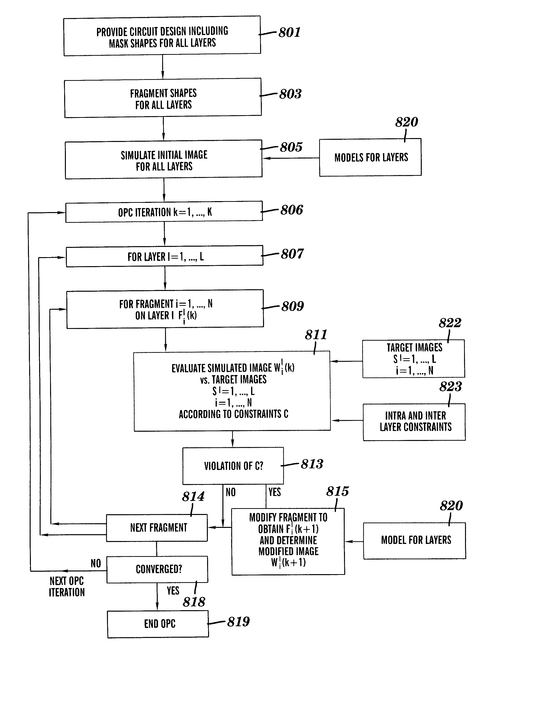
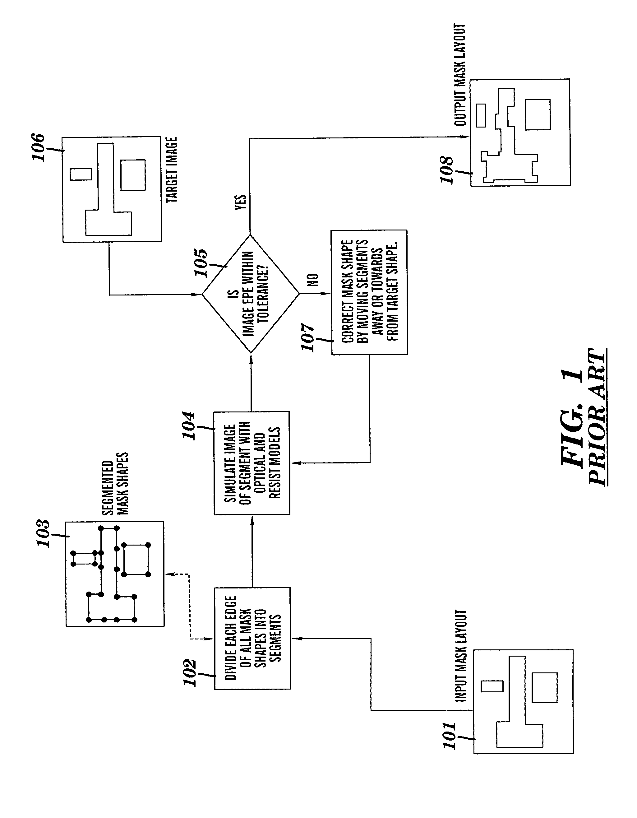
[0040] The present invention is ultimately used in optical lithography to correct for any distortions on a photo-mask having patterns of circuit design features, in order to achieve a projection thereof on the photo-resist coated wafers, such that the proper functionality of the circuit is ensured. In accordance with the present invention, model-based OPC is performed in which conventional edge-placement error (EPE) constraints are relaxed or replaced with intra-layer and inter-layer constraints and specifications that ensure proper interaction among more than one layer.
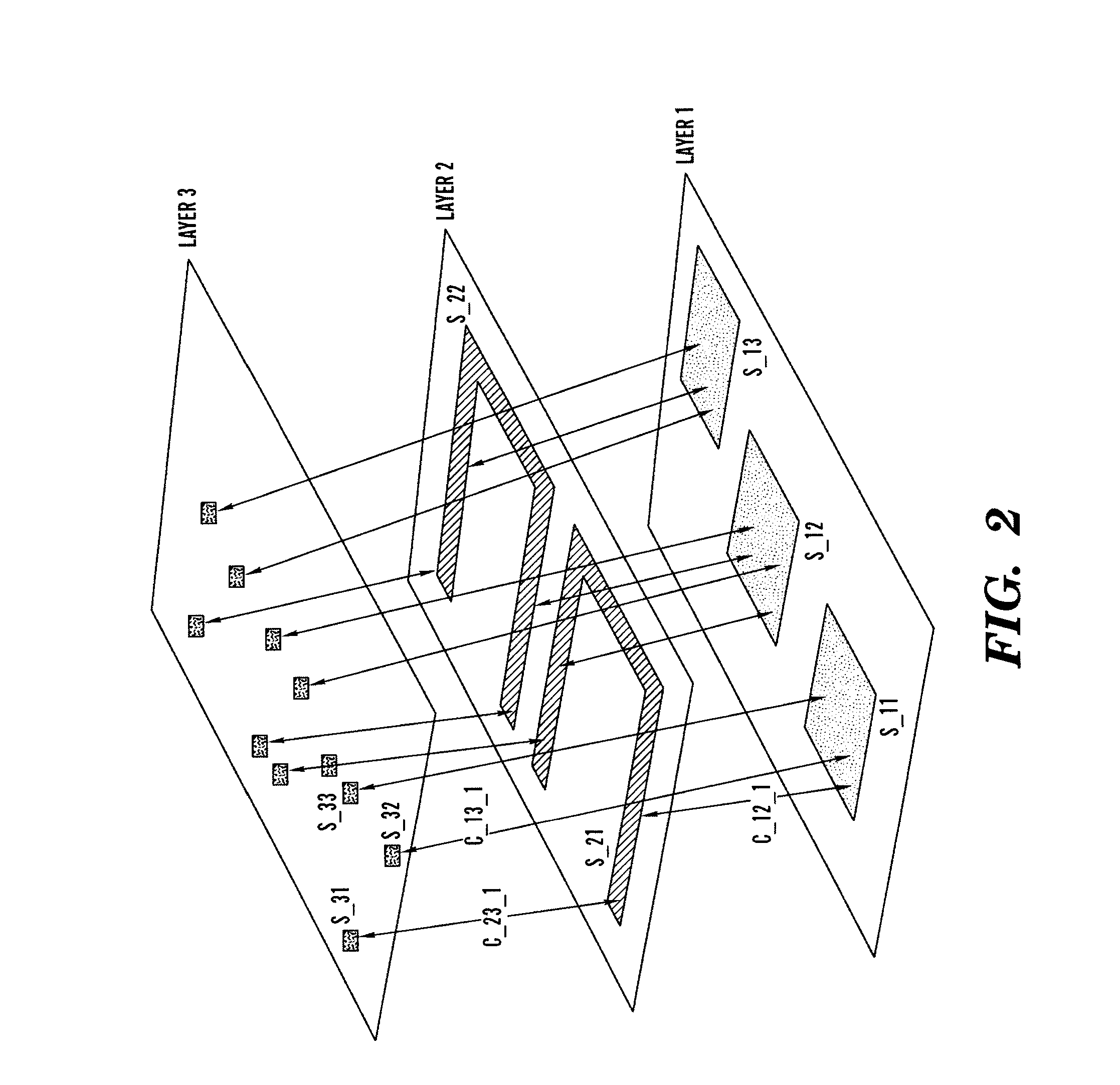
[0041] Referring to FIG. 2, the relationship among several layers is illustrated. Here we have shown three layers, viz., Layer 1, Layer 2 and Layer 3. The mask layouts corr...
PUM
 Abstract
Description
Claims
Application Information