Flash memory

a flash memory and flash technology, applied in the field of flash memory, can solve problems such as data destruction, computer system crash, and data loss, and achieve the effect of high reliability

Inactive Publication Date: 2007-09-27
TOSHIBA MEMORY CORP
View PDF3 Cites 100 Cited by
  • Summary
  • Abstract
  • Description
  • Claims
  • Application Information

AI Technical Summary

Benefits of technology

[0018] (2) The flash memory, which can shorten an appearance read time and can shorten an average read time by shortening the time required to detect an error and to specify the error.
[0117] According to the twenty-first flash memory, the information data written in the predetermined memory cell is replaced with fixed data and the check data is generated, in error correction circuit. In this case, the information data and the check data are temporarily memorized in a plurality of data memory circuits, which are provided to each memory cell, and are written in the memory cell in a lump. In the data memory circuit, the memorized data is reset to fixed data before inputting the information data. Therefore, the flash memory, which has a simple and fast circuit and can correctly perform the error correction without depending on the data length, can be provided.

Problems solved by technology

Therefore, when only one bit error is occurred in the data memorized in the flash memory, crash of the computer system, disable of communication of a portable telephone and destroy of data will be occurred.
However, there are many cases that the methods of the error correction are different for each system, which manages the flash memories.
That is, when the data written by a certain system A is read with another system B, even when there is no error in data, correct data is changed as it is assumed that data has an error, misdetection of error which is not able to be corrected, as a result, the destruction of data in the system will occur.
However, since the error correction circuit is complex and the area of the circuit becomes large, the size of the chip of the flash memory becomes large, as a result, the high cost will be caused.
However, in the flash memory of the multi-level memory, when one memory cell destroys, the error is caused in the data of two or more bits (that is, the burst error is caused).
To correct such a burst error efficiently by short check data, though there is a method of the error correction based on the Reed-Solomon code, a complex circuit is required to specify the error, the area of the circuit becomes large, the size of the chip of the flash memory becomes large, and the high cost will be caused.

Method used


Image

  • Flash memory
  • Flash memory
  • Flash memory

Examples


first embodiment

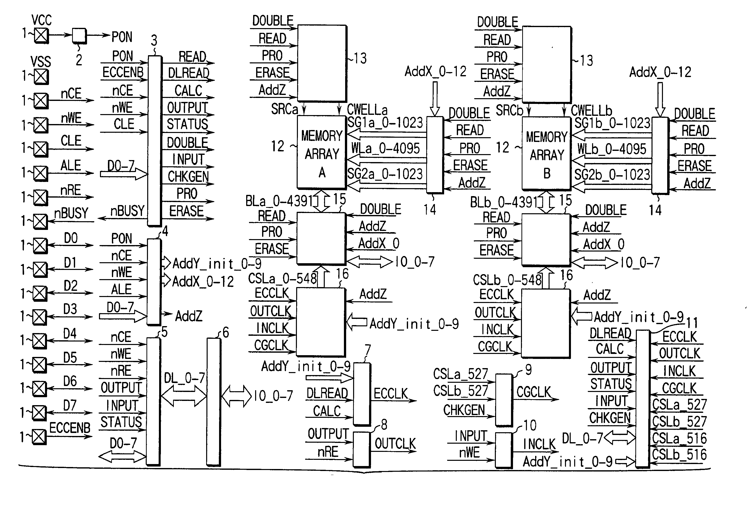
[0147]FIG. 1 is a block diagram, which shows the configuration of the flash memory according to the first embodiment of the present invention.

[0148] A plurality of terminals 1 are provided to receive the power supply and the signal from the external device or to output the signal to the external device. Among these terminals 1, the VCC terminal receives power-supply voltage VCC, the VSS terminal is grounded, the nCE terminal receives chip enable signal nCE, the nWE terminal receives write enable signal nWE, the CLE terminal receives command latch enable signal CLE, the ALE terminal receives address latch enable signal ALE, the nRE terminal receives read enable signal nRE, and the ECCENB terminal receives error correction circuit activation signal ECCENB.

[0149] The terminal nBUSY outputs busy signal nBUSY, and D0 terminal to D7 terminal receive input data D0 to D7 such as the write data, the command data, and the address data and output output data D0 to D7 such as the read data an...

second embodiment

[0302] The second embodiment differs from the first embodiment only in read operation.

[0303] The circuit configuration of the flash memory, which equips the error correction circuit, according to the second embodiment is almost similar to the circuit configuration shown in FIG. 1, and, in addition, the point to receive the error correction instruction from the external device and output error correction read instruction signal ECREAD from the command interface 3 is different.

[0304]FIG. 23 shows an example of algorithm, which performs the error position detection and correction from the read data with error correction circuit 11 of the FIG. 1, in the second embodiment, and differs from the algorithm, which performs the error position detection and correction from the read data with error correction circuit 11 of the FIG. 1, in the first embodiment referring to FIG. 18.

[0305] That is, first, the memory sector and the start column address data, which starts reading, is input (step S...


PUM


Abstract

A flash memory includes a memory sector, a command interface, a first signal buffer, a control signal generation circuit, a data input buffer, an error correction circuit, an address buffer, an address signal generation circuit, a plurality of data memory circuits, and write circuit. The command interface receives a write data input instruction from an external device to generate a write data input instruction signal, and receives a write instruction from the external device to generate a write instruction signal. The error correction circuit is activated by the write data input instruction signal to receive the write data in synchronization with the write enable signal, and is activated by the write instruction signal to generate a check data for an error correction in synchronization with the control signal.

Description

CROSS-REFERENCE TO RELATED APPLICATIONS [0001] This application is a Divisional of U.S. application Ser. No. 10 / 601,636 filed Jun. 24, 2003, which is a Divisional of U.S. application Ser. No. 09 / 604,692 filed on Jun. 27, 2000, which is based upon and claims the benefit of priority from the prior Japanese Patent Application No. 11-181874, filed Jun. 28, 1999, the entire contents of which are incorporated herein by reference.BACKGROUND OF THE INVENTION [0002] The present invention relates to a flash memory, especially, to a flash memory, which comprises an error correction circuit and has high reliability, and to a flash memory used for such as NAND type flash memory and NOR type flash memory. [0003] Among the nonvolatile semiconductor memories, the flash memory can electrically erase and rewrite data for a comparatively large unit. Then, the flash memory is applied to the memory of BIOS (basic I / O system) in the computer system, the memory of the communication rule etc. in a portable...

Claims


Application Information

Patent Timeline
Patent Type & Authority Applications(United States)
IPC IPC(8): G11C16/06G11C17/00G06F11/10G11C16/00G11C29/42
CPCG06F11/1008G06F11/1068G06F11/1072G11C7/1006G06F11/10G11C16/10G11C2029/0411G11C2207/104G11C16/0483G11C16/00
Inventor TANAKA, TOMOHARUSHIBATA, NOBORUTANZAWA, TORU
Owner TOSHIBA MEMORY CORP
Why Eureka
Try Eureka