Superluminescent diode and method of manufacturing the same

a superluminescent diode and superluminescent light technology, applied in semiconductor lasers, laser details, electrical apparatus, etc., can solve the problem that the sld cannot generate an optical power greater than 20 mw, and achieve the effect of high power and broadband characteristics

Active Publication Date: 2007-09-27
ELECTRONICS & TELECOMM RES INST
View PDF8 Cites 17 Cited by
  • Summary
  • Abstract
  • Description
  • Claims
  • Application Information

AI Technical Summary

Benefits of technology

[0018] According to the present invention, the 1.55 μm SLD may be manufactured by forming two electrodes for the SOA and LD at the sa

Problems solved by technology

Since an injection current of less than 200 mA is supplied to SLDs for optical communi

Method used


Image

  • Superluminescent diode and method of manufacturing the same
  • Superluminescent diode and method of manufacturing the same
  • Superluminescent diode and method of manufacturing the same

Examples


Embodiment Construction

[0024] The present invention will now be described more fully with reference to the accompanying drawings, in which exemplary embodiments of the invention are shown.

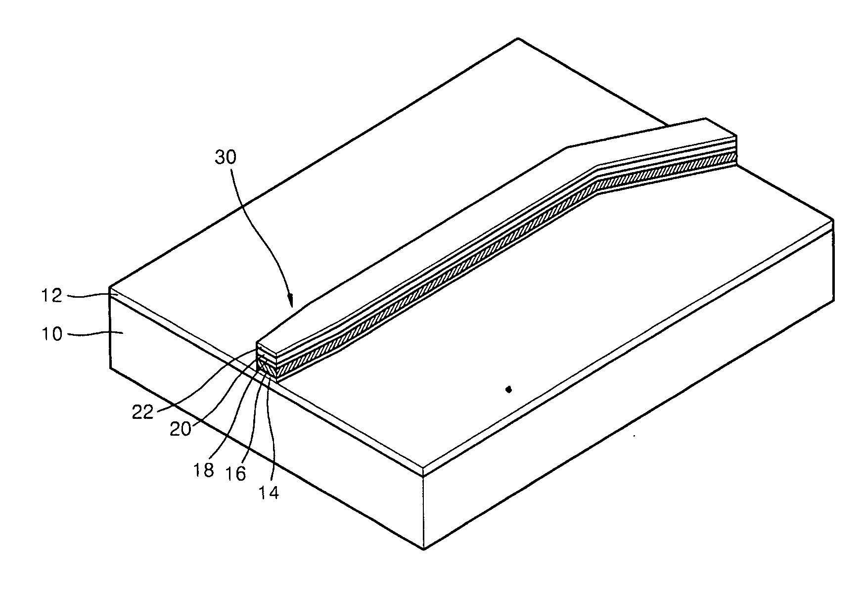
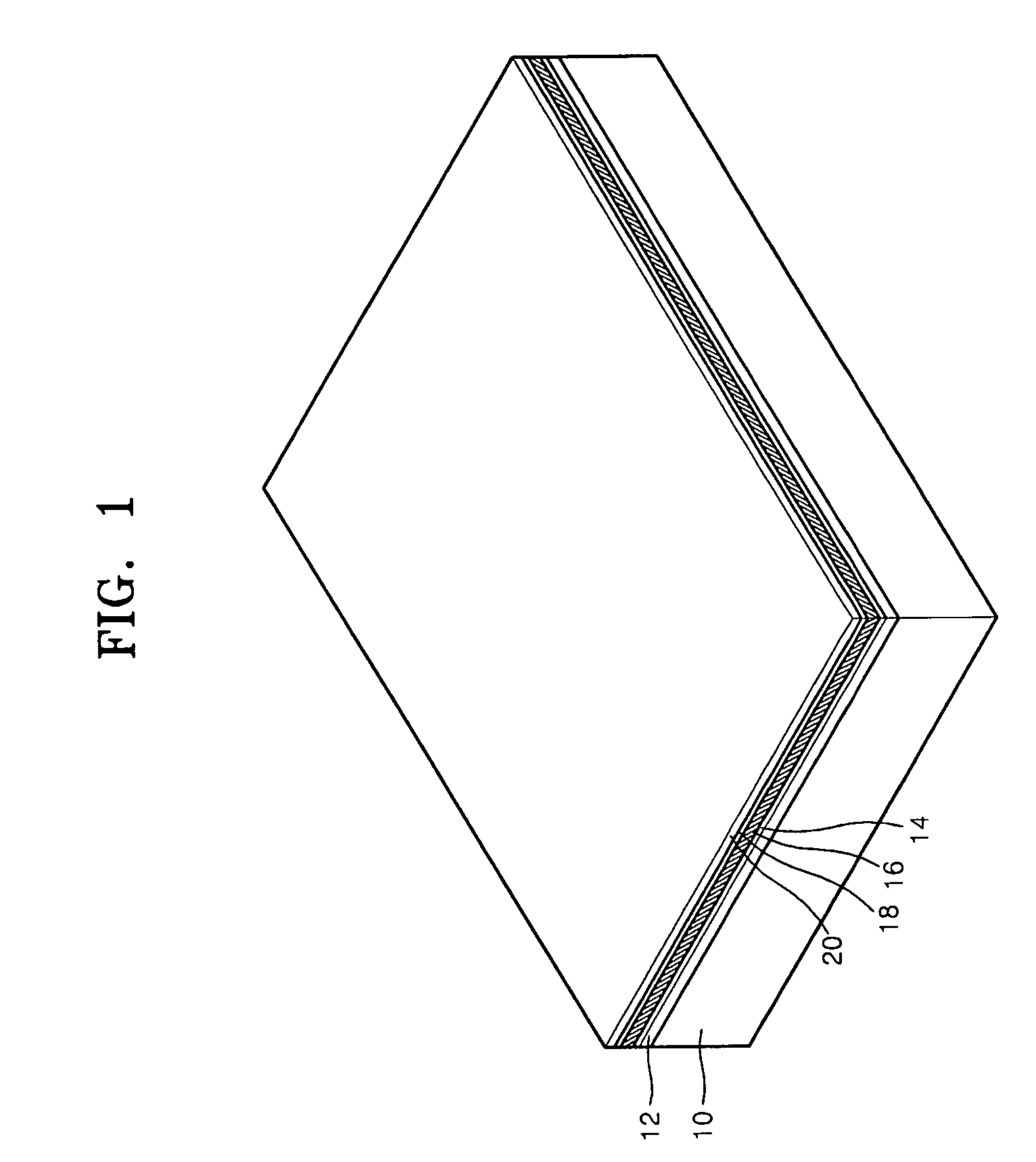
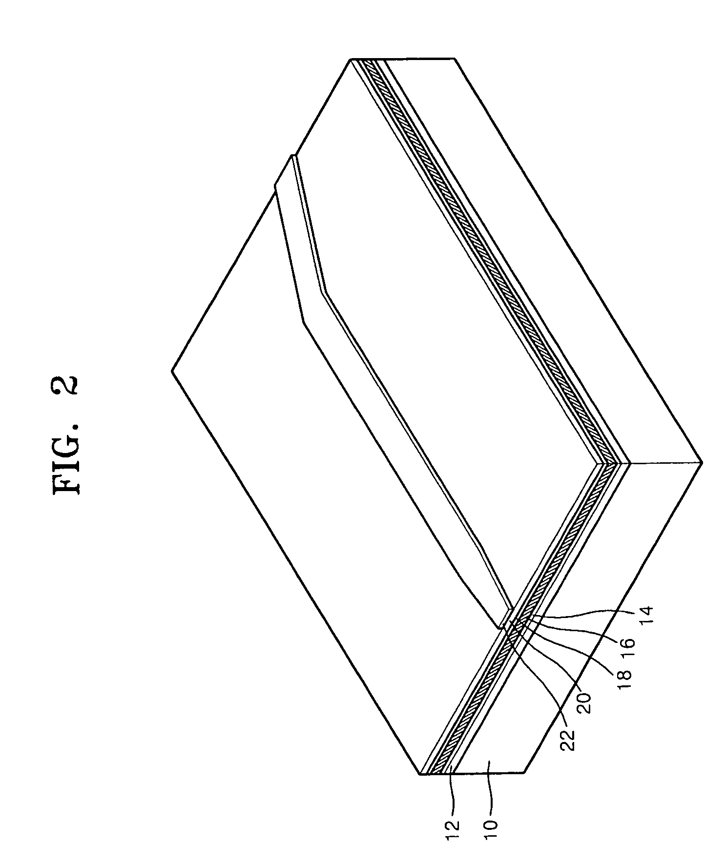
[0025]FIGS. 1 through 9 are perspective views of an SLD for describing a method of manufacturing a superluminescent diode (SLD) according to an embodiment of the present invention.

[0026] Referring to FIG. 1, an InP buffer layer 12 (λ=1.3 μm and thickness=0.3 μm) and a first separate confinement hetero-structure layer (SCH) layer 14 (λ=1.3 μm and thickness=0.07 μm) are sequentially formed on an n-InP substrate 10 by metal organic chemical vapor deposition (MOCVD).

[0027] An active layer 16 is then formed on the first SCH layer 14. For example, a multi-quantum well (MQW) can be formed by alternately depositing unstrained InGaAsP barriers (λ=1.68 μm and thickness=11.5 nm) and 0.8% InGaAsP strained well layers (λ=1.3 μm and thickness=7 nm) several times. For example, the active layer 16 can be formed by depositing seven pa...


PUM


Abstract

A 1.55 μm SLD having a laser diode (LD) region and a semiconductor optical amplifier (SOA) region, and a method of fabricating the same, are disclosed. The SLD includes: an InP substrate having a LD region and a SOA region for amplifying light emitted from the LD region; an optical waveguide having a BRS (buried ridge strip) structure having an active layer of resonant strip pattern formed on the InP substrate and extending from the SOA region to the LD region; a first electrode formed on the active layer in the SOA region, a second electrode formed on the active layer in the LD region and electrically isolated from the first electrode; and a current blocking region interposed between the first electrode and the second electrode in order to electrically isolate the first electrode and the second electrode from each other.

Description

CROSS-REFERENCE TO RELATED PATENT APPLICATION [0001] This application claims the benefit of Korean Patent Application No. 10-2005-0121981, filed on Dec. 12, 2005, in the Korean Intellectual Property Office, the disclosure of which is incorporated herein in its entirety by reference. BACKGROUND OF THE INVENTION [0002] 1. Field of the Invention [0003] The present invention relates to a high power semiconductor light source and a method of manufacturing the same, and more particularly, to a superluminescent diode (SLD) which emits light of 1.55 μm wavelength, and a method of manufacturing the same. [0004] 2. Description of the Related Art [0005] Conventional light sources for optical communication, optical measurement and bio-imaging generally emit visible light or light of 1.3 μm wavelength. There has been very little research into a superluminescent diode (SLD) which emits light of 1.55 μm wavelength, until now. [0006] Conventional structures for suppressing laser oscillation of an S...

Claims


Application Information

Patent Timeline
IPC IPC(8): H01S5/00
CPCB82Y20/00H01S5/026H01S5/0265H01S5/0425H01S5/101H01S5/4006H01S5/2201H01S5/2224H01S5/2275H01S5/3406H01S5/34306H01S5/2063H01S5/04256
Inventor PARK, MOON HOBAEK, YONG SOONOH, KWANG RYONG
Owner ELECTRONICS & TELECOMM RES INST
Why Eureka
Try Eureka