

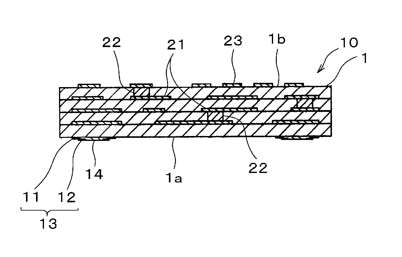
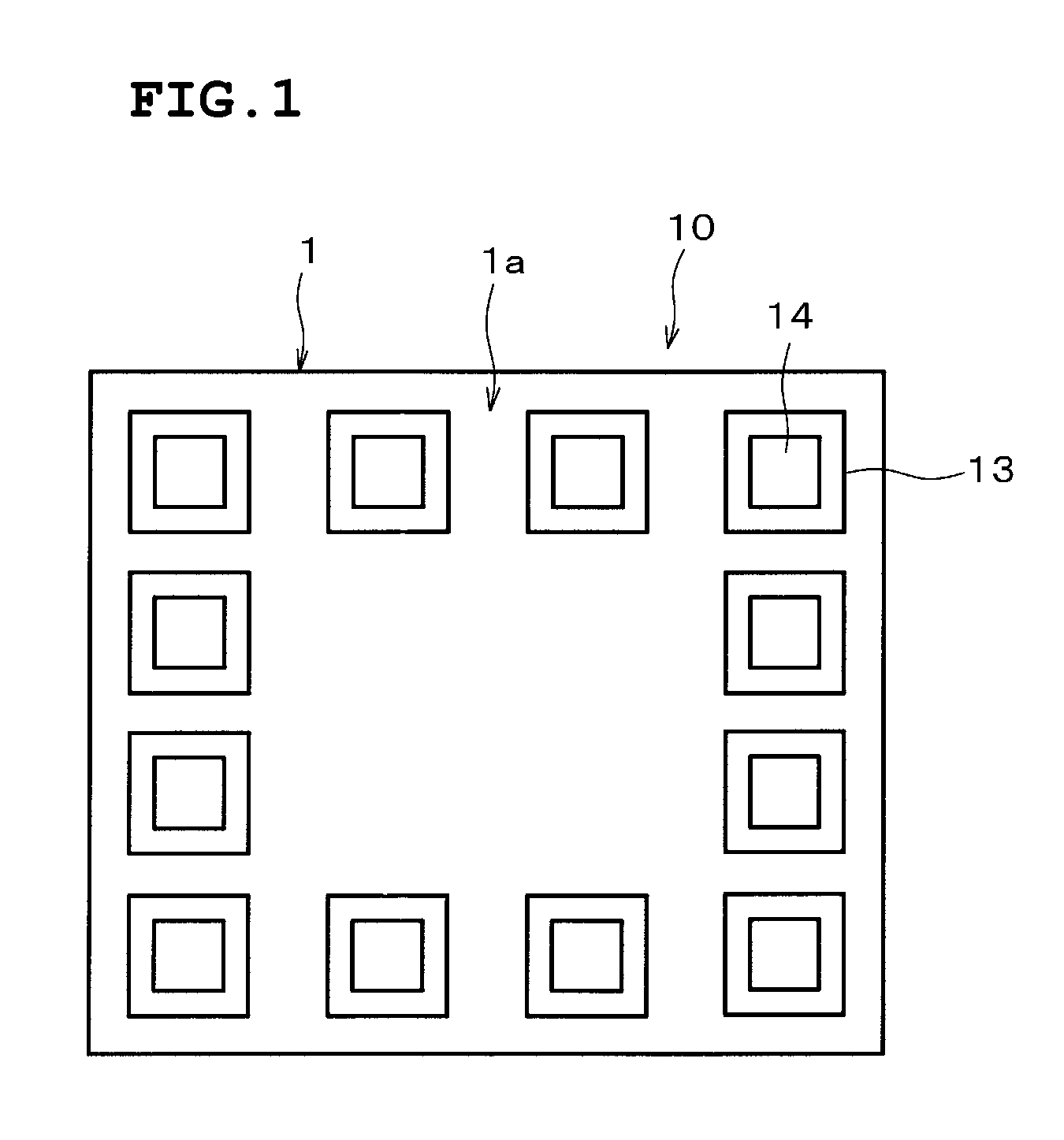
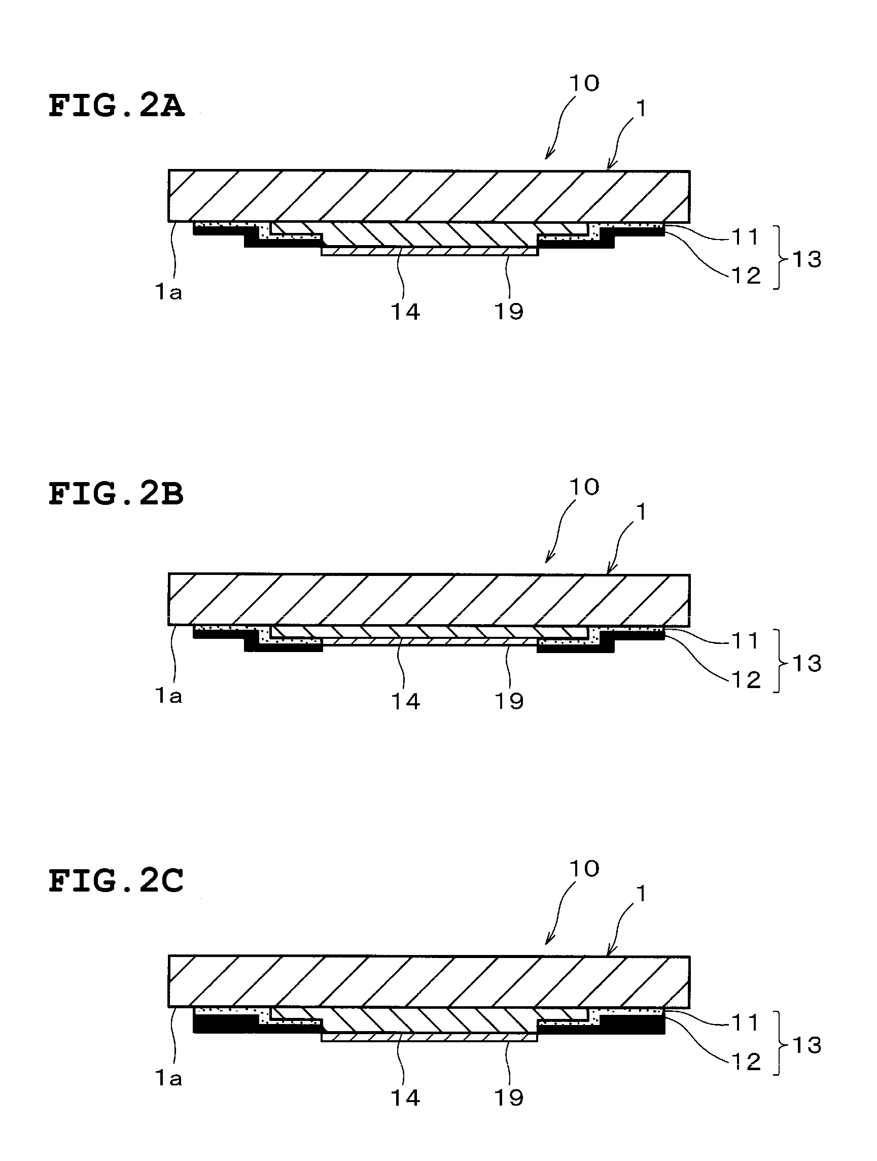
Ceramic substrate, electronic apparatus, and method for producing ceramic substrate
a ceramic substrate and electronic equipment technology, applied in the direction of electrical equipment casings/cabinets/drawers, hermetically sealed casings, semiconductor/solid-state device details, etc., can solve problems such as pinholes, and achieve superior plating resistance, superior adhesion, and high reliability
- Summary
- Abstract
- Description
- Claims
- Application Information
AI Technical Summary
Benefits of technology
Problems solved by technology
Method used
Image

Examples
embodiment 1
Preferred Embodiment 1
[0049] A method for producing a ceramic substrate according to a preferred embodiment of the present invention will be described below.
Production of Ceramic Substrate
[0050] Equal weights of an alumina powder and a crystallized-glass powder obtained by mixing SiO2, Al2O3, B2O3, and CaO were mixed to form a mixed powder.
[0051] To 100 parts by weight of the resulting mixed powder, 15 parts by weight of polyvinyl butyral, 40 parts by weight of isopropyl alcohol, and 20 parts by weight of toluol(toluene) were added, and then the mixture was mixed for about 24 hours with a ball mill to form a slurry.
[0052] The resulting slurry was formed into ceramic green sheets each having a thickness of about 120 μm by a doctor blade method.
[0053] As a substrate for a heat cycle evaluation, through holes for interlayer connection were formed in each of the resulting ceramic green sheets. The through holes were filled with a conductive paste. A conductive paste was applied to...
PUM
| Property | Measurement | Unit |
|---|---|---|
| thickness | aaaaa | aaaaa |
| thickness | aaaaa | aaaaa |
| thickness | aaaaa | aaaaa |
Abstract
Description
Claims
Application Information