
Method of manufacturing display device using LED chips

a technology of led chips and display devices, applied in the field of manufacturing a display device, can solve the problems of high manufacturing cost, low yield, and high process temperature requirements

Active Publication Date: 2007-09-27
SAMSUNG DISPLAY CO LTD
View PDF18 Cites 51 Cited by
  • Summary
  • Abstract
  • Description
  • Claims
  • Application Information

AI Technical Summary

Benefits of technology

[0007] It is therefore, an object of the present invention to provide an improved method for manufacturing display devices using light emitting diode (LED) chips.
[0009] It is still another object to provide a less expensive method for the manufacture of display devices using light emitting diode (LED) chips.
[0010] These and other objects may be attained according to the principles of the present invention to manufacture display devices that use light emitting diode (LED) chips more simply, at lower costs by manufacturing the LED chips with a porous template.

Problems solved by technology

In this method however, manufacturing costs are high, yield is low, and high process temperatures are required.

Method used


Image

  • Method of manufacturing display device using LED chips
  • Method of manufacturing display device using LED chips
  • Method of manufacturing display device using LED chips

Examples


Embodiment Construction

[0031] The present invention will now be described more fully with reference to the accompanying drawings, in which an exemplary embodiment of the invention are shown. Like reference numerals in the drawings denote like elements.

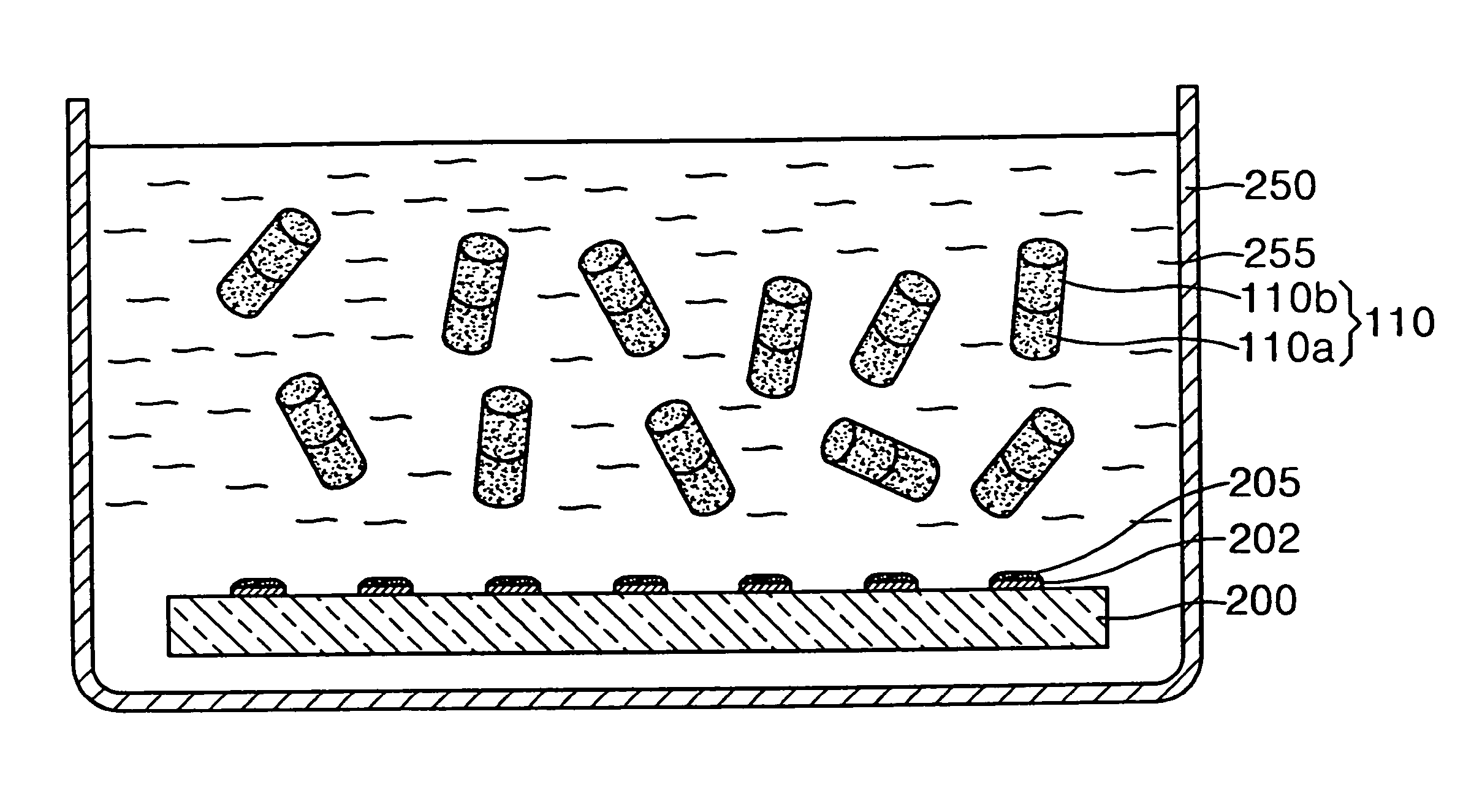
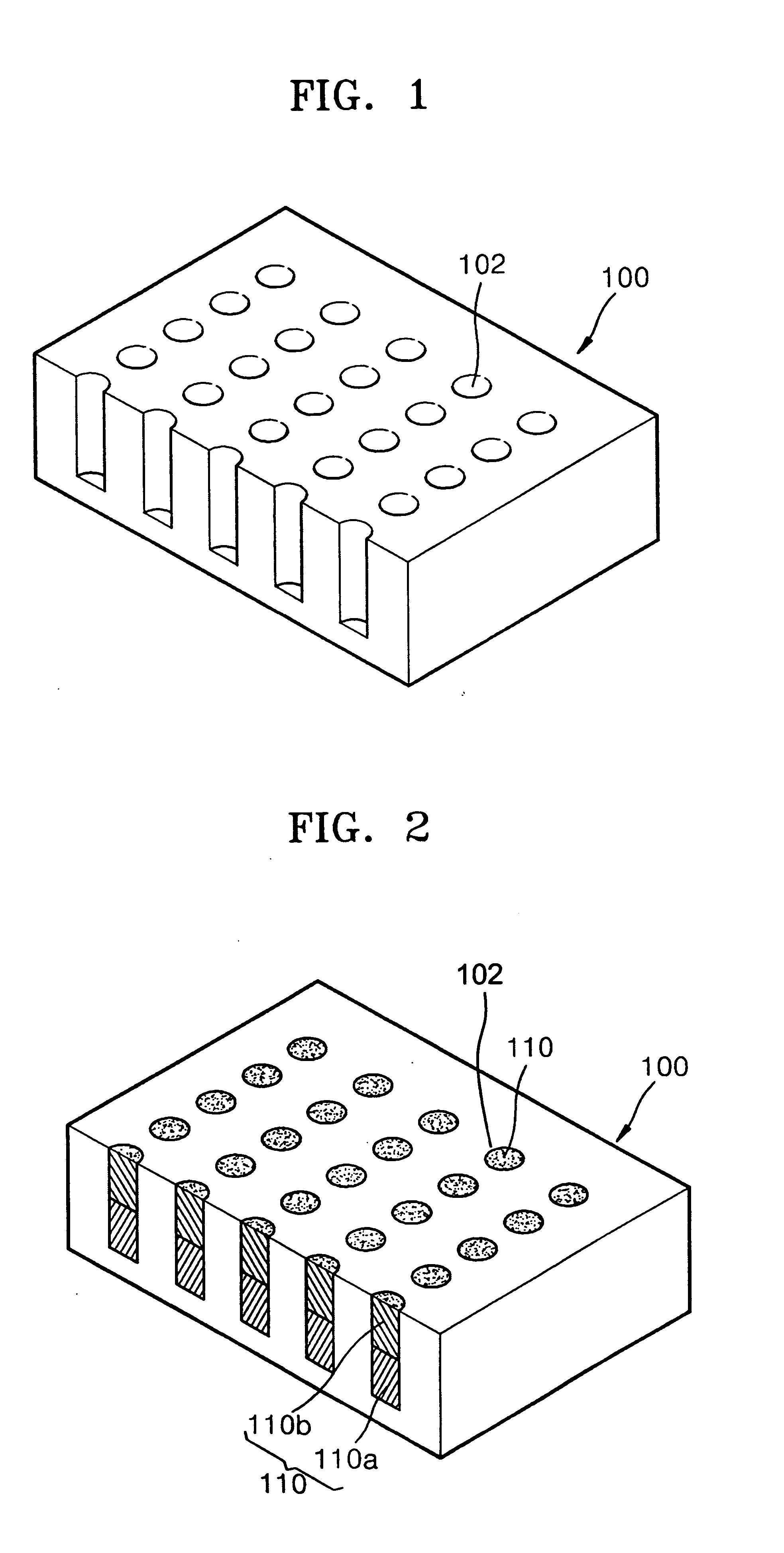
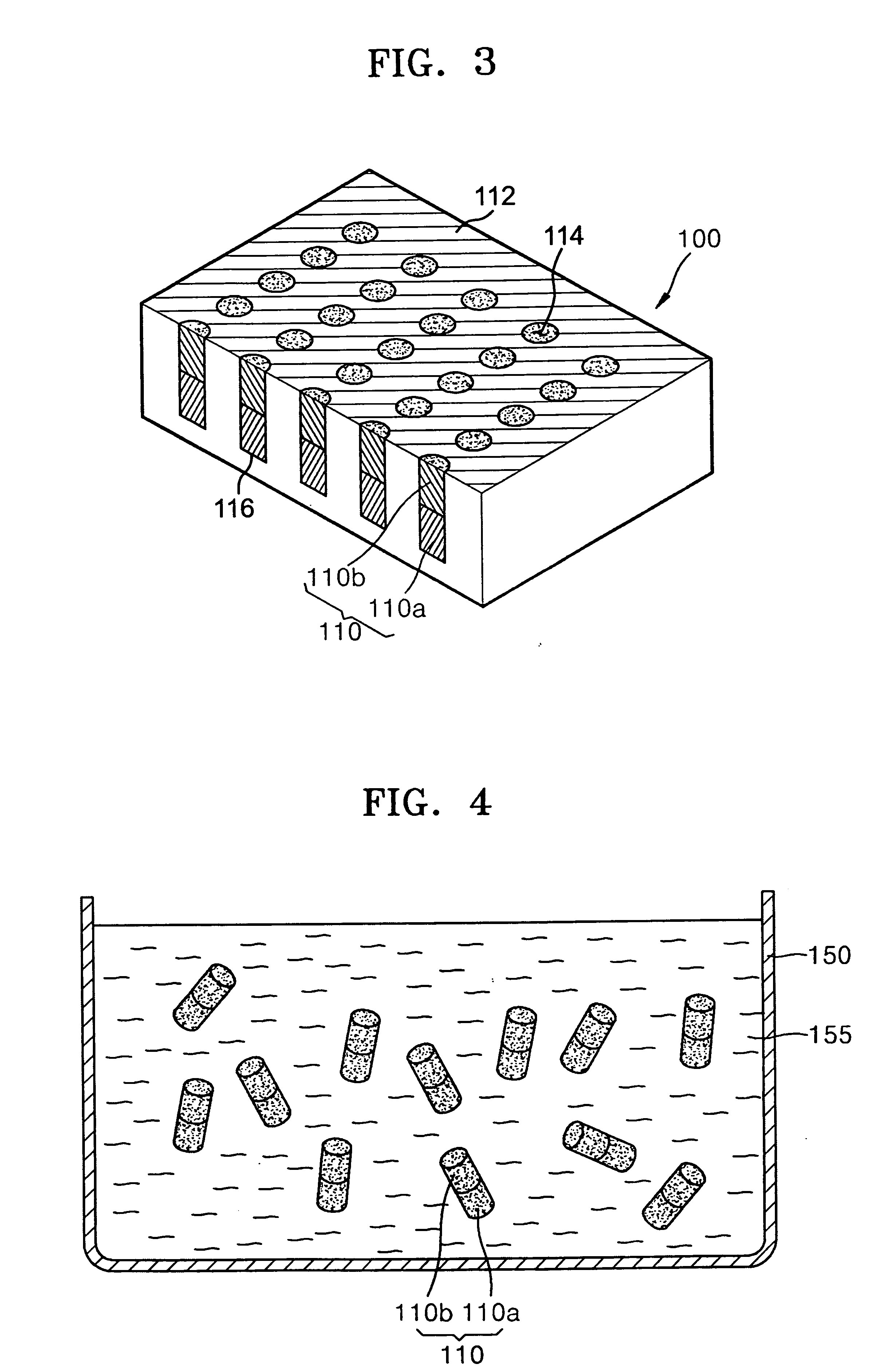
[0032]FIGS. 1 through 12 illustrate a method of manufacturing a display device using light emitting diode (LED) chips according to an embodiment of the present invention. FIGS. 1 through 4 illustrate a process of manufacturing LED chips.

[0033] Referring now to FIG. 1, a porous template 100 is prepared in which pores 102 (e.g., blind holes opening on one major surface of template 100) with predetermined cross-sectional dimensions and depths are formed. Here, porous template 100 may be formed from anodized aluminum oxide or porous glass fiber, etc. The size of pores 102 may be set to different dimensions according to conform with the size of the LED chips. For example, pores 102 may have a diameter within a range of about 1 nm to about 100 μm.

[0034] Referri...


PUM


Abstract

A method for manufacturing a display device using light emitting diode chips contemplates manufacturing a plurality of light emitting diode (LED) chips using a porous template; forming a plurality of first electrodes on a substrate; attaching the LED chips to pixel sites on the first electrodes using fluidic self assembly (FSA); and forming a plurality of second electrodes on a top surface of the LED chips.

Description

CLAIM OF PRIORITY [0001] This application makes reference to, incorporates the same herein, and claims all benefits accruing under 35 U.S.C. §119 from an application earlier filed in the Korean Intellectual Property Office on Mar. 21, 2006 and there duly assigned Serial No. 10-2006-0025673. BACKGROUND OF THE INVENTION [0002] 1. Field of the Invention [0003] The present invention relates to a method of manufacturing a display device, and more particularly, to a method of simplifying the manufacture of display devices using light emitting diode (LED) chips while reducing the costs of manufacture. [0004] 2. Description of the Related Art [0005] Light emitting diodes (LEDs) are devices which transform electric energy into light. LEDs are used in illumination, as backlighting units in liquid crystal displays (a LCD), and in display devices projecting variable visual images to viewers, as for example, in a video display device such as a monitor. [0006] Display devices using LED chips are ...

Claims


Application Information

Patent Timeline
IPC IPC(8): H01L21/00
CPCH01L24/95H01L25/50H01L2224/95085H01L2224/95122H01L2924/01013H01L2924/01015Y10S977/883H01L2924/01005H01L2924/01006H01L2924/01033H01L2224/83192Y10S977/949H01L2924/01049H01L2924/12041H01L2924/00A01G13/0237A01G13/0281
Inventor HAN, IN-TAEKKIM, JONG-MIN
Owner SAMSUNG DISPLAY CO LTD
Features
  • Generate Ideas
  • Intellectual Property
  • Life Sciences
  • Materials
  • Tech Scout
  • Unparalleled Data Quality
  • Higher Quality Content
  • 60% Fewer Hallucinations
Learn More