Apparatus and method for manufacturing a display device substrate
- Summary
- Abstract
- Description
- Claims
- Application Information
AI Technical Summary
Benefits of technology
Problems solved by technology
Method used
Image
Examples
first embodiment
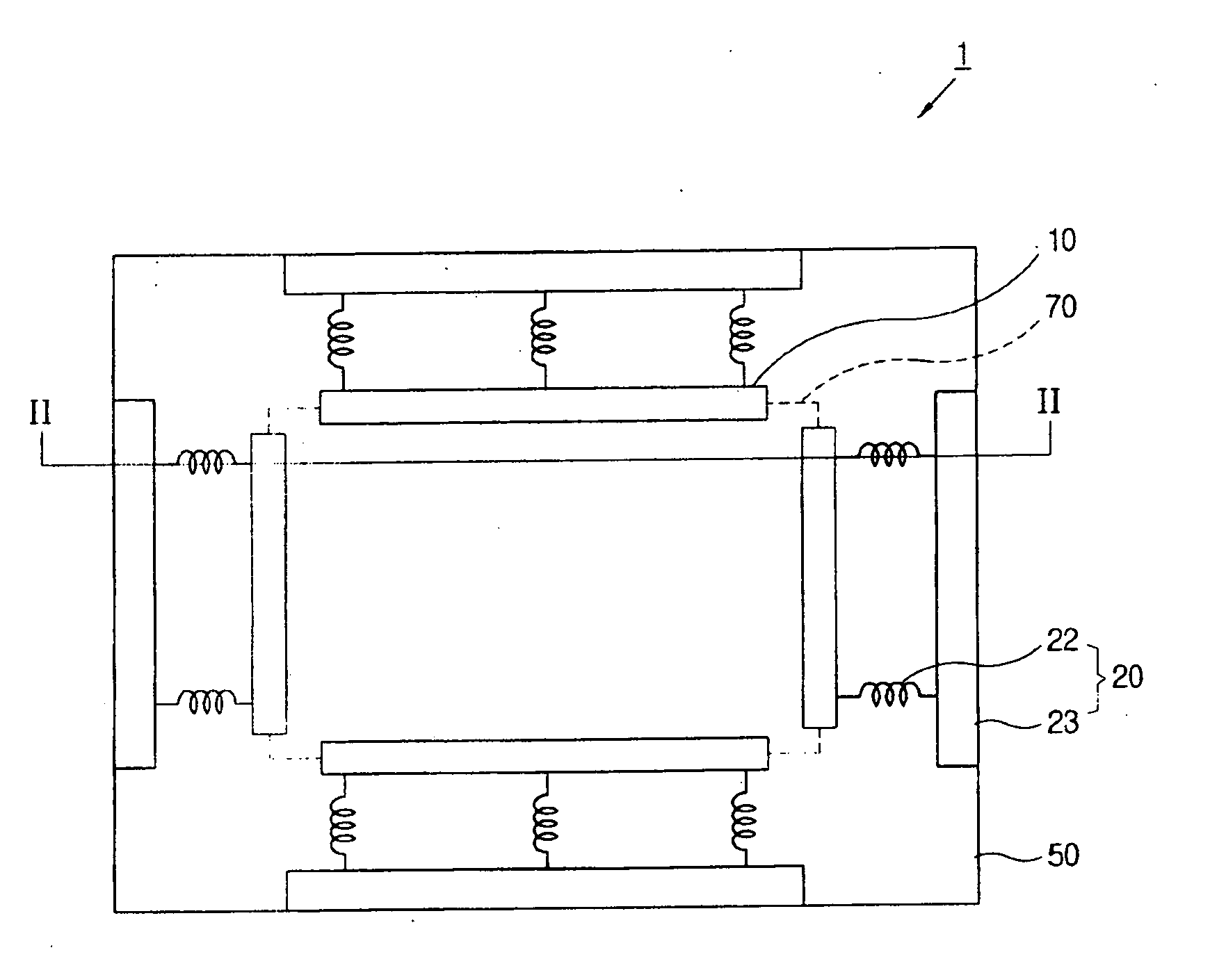
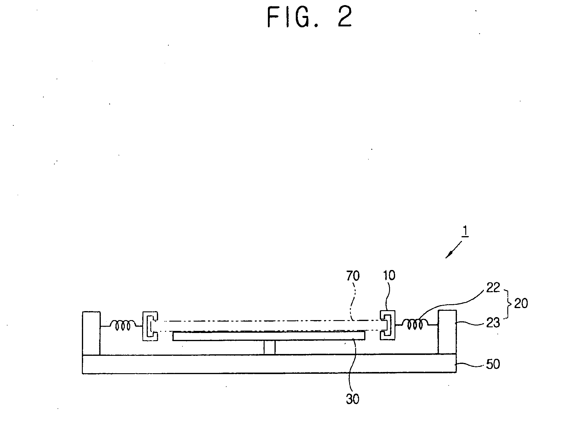
[0040]FIG. 1 is a plane view of an apparatus for manufacturing a display device substrate according to the present invention, and FIG. 2 is a sectional view of the apparatus for manufacturing a display device substrate, taken along line II-II in FIG. 1.
[0041] Referring now to FIGS. 1 and 2, an apparatus 1 for manufacturing a display device substrate according to a first embodiment of the invention includes a clamp 10, a tension member 20, an electrostatic chuck 30, and a base plate 50.
[0042] A plurality of clamps 10 clamp four sides of a plastic substrate 70, which is a base substrate of the display device substrate, to apply tension along a surface of the plastic substrate 70 while interacting with the tension member 20. In one example, the clamp 10 may be made of stainless steel, which is strong, or in another example, synthetic resins, which do not react to the plastic substrate 70. The clamp 10 is formed in a bar shape in a further example. One clamp 10 may clamp the majority o...
second embodiment
[0057] An apparatus 2 for manufacturing the display device substrate according to the present invention includes a tension member 25 comprising a tension unit 26 made of an electromagnet and a support part 27 supporting the tension unit 26. A clamp 11, made of a ferromagnetic metal, in one example, is attracted to the electromagnet. The ferromagnetic metal may include at least one of iron, nickel, and cobalt. Also, the apparatus for manufacturing the display device substrate 2 includes an electric current providing unit 40 which provides an electric current to the magnetic field, which allows for the interaction between the clamp 11 and a substrate 70.
[0058] Thus, the tension unit 26 generates the tension between the tension member 25 and the clamp 11 though not directly contacting with the clamp 11, and the tension is applied along a surface of the plastic substrate 70, thereby reducing deflection of the plastic substrate 70.
[0059] A method for manufacturing a display device subst...
PUM
 Abstract
Description
Claims
Application Information


