Apparatus and method of static timing analysis considering the within-die and die-to-die process variation

a static timing analysis and apparatus technology, applied in the field of semiconductor methods and apparatuses, can solve the problems of increasing manufacturing variation, reducing the yield of semiconductor integrated circuits, and reducing the so as to reduce power consumption and chip area, and calculate quickly and precisely

Inactive Publication Date: 2007-09-27
PANASONIC CORP
View PDF5 Cites 20 Cited by
  • Summary
  • Abstract
  • Description
  • Claims
  • Application Information

AI Technical Summary

Benefits of technology

[0017]It is therefore an object of the present invention to provide an apparatus and method for designing a semiconductor integrated circuit capable of quickly and precisely calculating fluctuation in the path delay time due to fluctuation in the semiconductor device manufacturing process.
[0018]It is also an object of the present invention to provide an apparatus and method for designing a semiconductor integrated circuit capable of quickly and precisely calculating a path delay worst value while appropriately taking into consideration how the range of path delay variation changes depending on the circuit configuration of the path.

Problems solved by technology

As the process rules for manufacturing semiconductor devices decrease, the increase in manufacturing variation has been a problem that needs to be addressed.
However, with a large-scale semiconductor integrated circuit, such a circuit simulation is not possible due to the large number of elements.
However, such a static timing analysis method is known to give an excessive estimate value with respect to the path delay worst value of an actually manufactured circuit due to the recent increase in manufacturing variation.
However, the delay times may actually be different from one another if there is an increased transistor local variation.
However, they still have problems as follows.
For example, with the statistical static timing analysis method as shown in Non-Patent Document 1, it is difficult to precisely calculate / express the range of delay variation for the cells, and it is therefore difficult to increase the precision with which the path delay variation is calculated.
Another problem is the increase in the calculation time as compared with conventional static timing analysis methods.
The method disclosed in Patent Document 1 also has the problem of increased calculation time.
Therefore, it is difficult to increase the precision with the method.
Moreover, it is not possible to determine the difference between a worst delay value calculated by the statistical static timing analysis method of Non-Patent Document 1 and that calculated by a conventional static timing analysis method.
Therefore, it is difficult for a designer to grasp the influence of the circuit dependency of the range of path delay variation due to process variation or to check whether or not there is erroneous input information.

Method used


Image

  • Apparatus and method of static timing analysis considering the within-die and die-to-die process variation
  • Apparatus and method of static timing analysis considering the within-die and die-to-die process variation
  • Apparatus and method of static timing analysis considering the within-die and die-to-die process variation

Examples


embodiment 1

[0095]A method and apparatus for designing a semiconductor integrated circuit according to according to a first embodiment of the present invention will now be described with reference to the drawings.

[0096]FIG. 1 is a block diagram showing an apparatus for designing a semiconductor integrated circuit of the present embodiment.

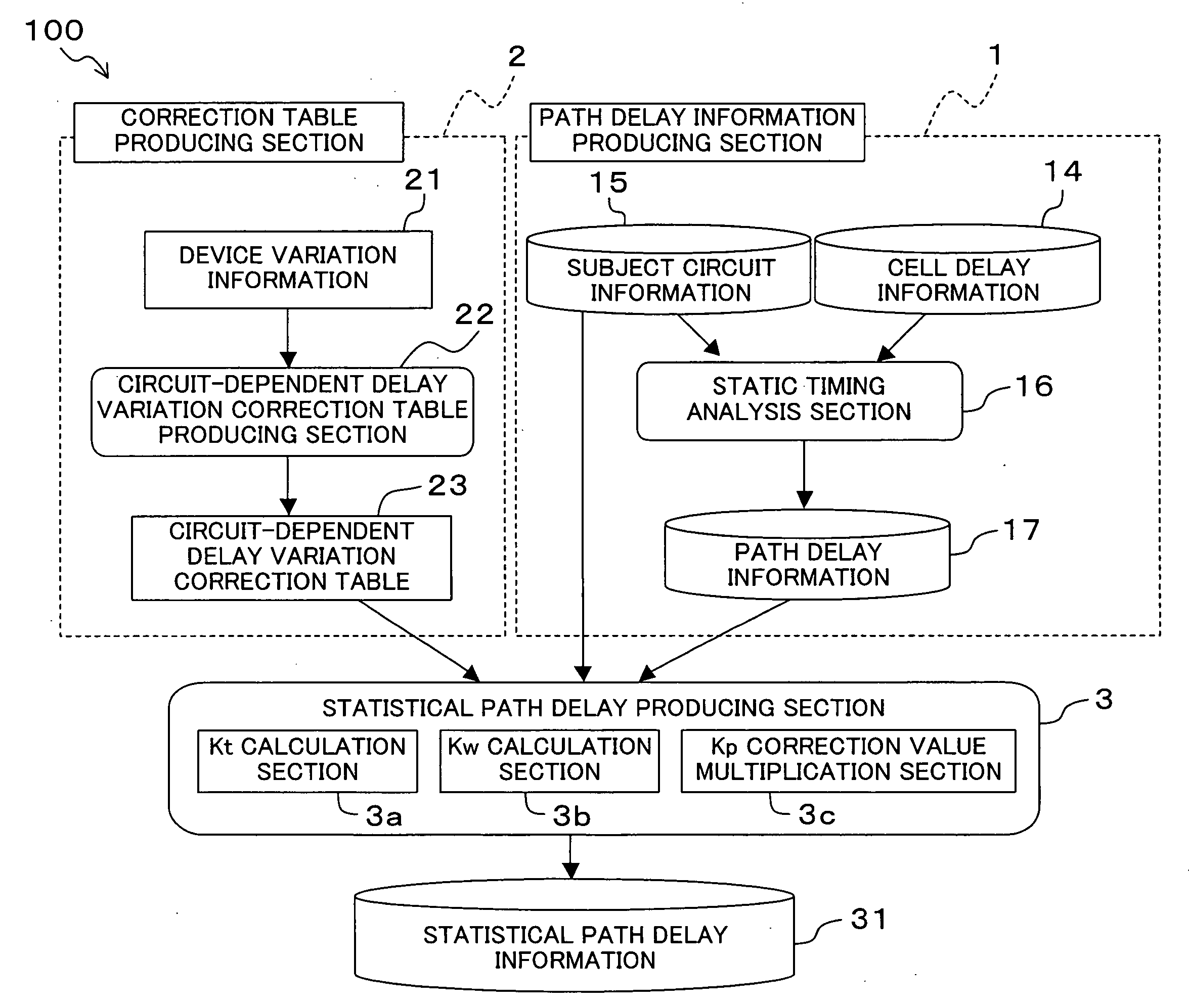
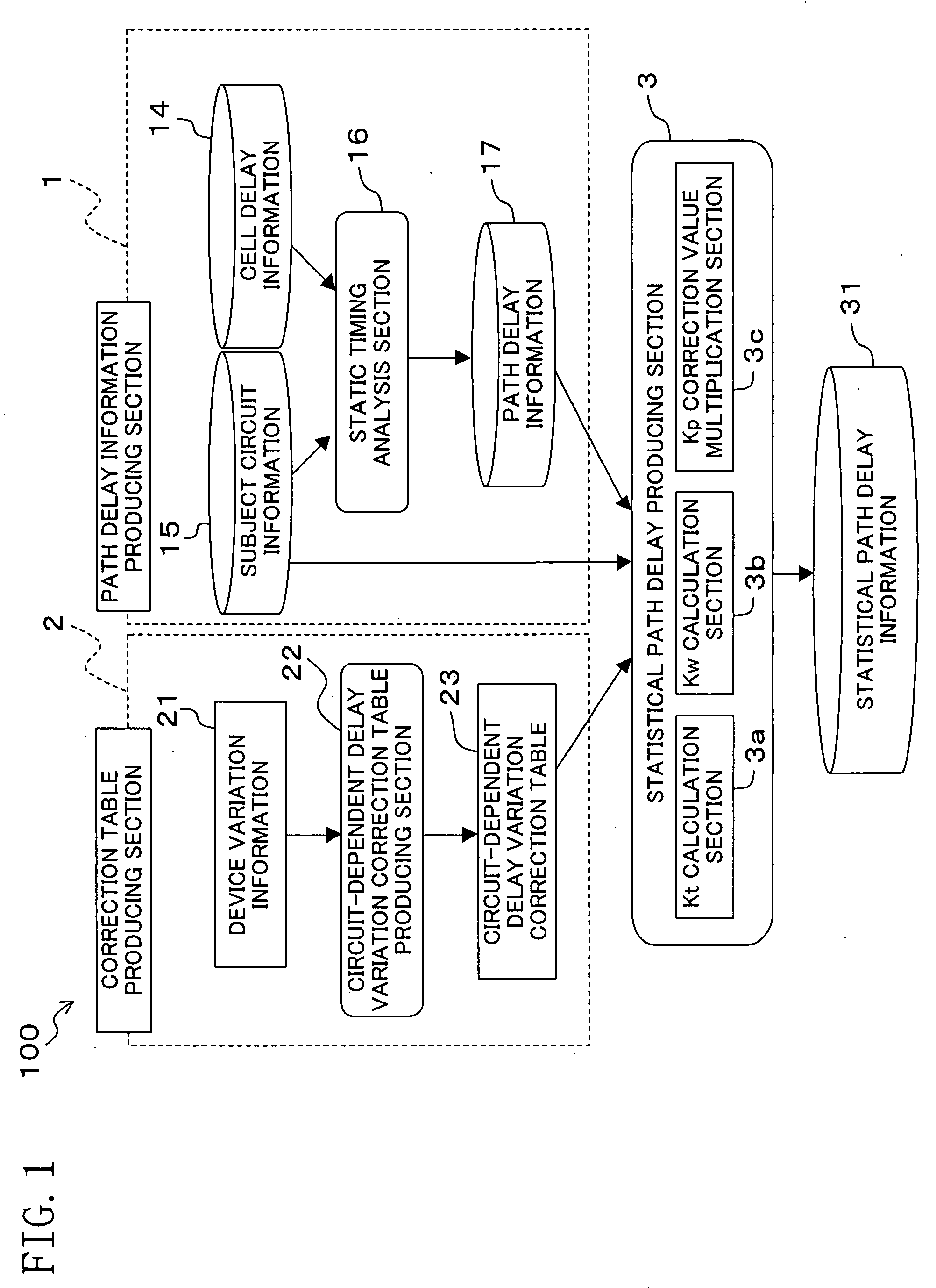
[0097]In FIG. 1, reference numeral 100 denotes a timing analysis device, 1 a path delay information producing section, 2 a correction table producing section, and 3 a statistical path delay producing section.

[0098]The path delay information producing section 1 includes a static timing analysis section 16 for producing path delay information 17 between registers, based on subject circuit information 15 and cell delay information 14, where the subject circuit information 15 represents how different cells are connected to one another and how parasitic elements, such as capacitors and resistors along wires between cells, are connected to one another, and the cell ...

embodiment 2

[0133]A method and apparatus for designing a semiconductor integrated circuit according to a second embodiment of the present invention will now be described with reference to the drawings.

[0134]FIG. 5 is a block diagram showing the apparatus for designing a semiconductor integrated circuit of the present embodiment. In the present embodiment, like elements to those of the first embodiment shown in the block diagram of FIG. 1 will be denoted by like reference numerals and will not be further described below.

[0135]An apparatus 101 for designing a semiconductor integrated circuit of the present embodiment includes a statistical maximum value calculation section 4 and a statistical maximum path delay information 32.

[0136]The operation up to when the statistical path delay information 31 is output is similar to that of the first embodiment and will not be further described below. The statistical maximum value calculation section 4 calculates, for each path, the range of path delay varia...

embodiment 3

[0139]A method and apparatus for designing a semiconductor integrated circuit according to a third embodiment of the present invention will now be described with reference to the drawings.

[0140]FIG. 6 is a block diagram showing the apparatus for designing a semiconductor integrated circuit of the present embodiment. In the present embodiment, like elements to those of the first embodiment shown in the block diagram of FIG. 1 will be denoted by like reference numerals and will not be further described below.

[0141]An apparatus 102 for designing a semiconductor integrated circuit of the present embodiment includes an arrangement and wiring section 41, a timing determination section 42 and a circuit modification section 43.

[0142]The arrangement and wiring section 41 reads out information on how connections are made in the semiconductor integrated circuit, and arranges and wires together cells, to thereby produce the subject circuit information 15. Based on the subject circuit informatio...


PUM


Abstract

In a method and apparatus for designing semiconductor integrated circuit, a path delay information producing section produces path delay information by performing a static timing analysis based on delay information of a cell and subject circuit information. A correction table producing section calculates circuit-dependent delay variation for each combination of circuit parameter values based on variation information of an element, and stores the calculated circuit-dependent delay variation in a delay correction table. A statistical path delay producing section calculates the circuit parameters for a path based on the subject circuit information and the path delay information, obtains the corresponding circuit-dependent delay variation based on the circuit-dependent delay variation correction table, and calculates and outputs statistical path delay information based on the circuit-dependent delay variation and the corresponding path delay information. Thus, it is possible to obtain a value close to an actual path delay worst value with only a little addition of calculation time.

Description

CROSS REFERENCE TO RELATED APPLICATION[0001]This Non-provisional application claims priority under 35 U.S.C. §119(a) on Patent Application No. 2006-081419 filed in Japan on Mar. 23, 2006, the entire contents of which are hereby incorporated by reference.BACKGROUND OF THE INVENTION[0002]The present invention relates to a method and apparatus for designing a semiconductor in which manufacturing variations are taken into consideration and which is capable of realizing a high performance and a high yield.[0003]As the process rules for manufacturing semiconductor devices decrease, the increase in manufacturing variation has been a problem that needs to be addressed. In designing a logic of a semiconductor integrated circuit, a synchronization circuit design method is mainly used in which a process is performed within a predetermined period of time by using a clock signal. In the synchronization circuit design method,T>Tpath+skew+setup   expression 1needs to be satisfied, where the cyc...

Claims


Application Information

Patent Timeline
Patent Type & Authority Applications(United States)
IPC IPC(8): G06F17/50
CPCG06F17/5031G06F30/3312
Inventor HIRATA, AKIO
Owner PANASONIC CORP
Why Eureka
Try Eureka