Piezoelectric driven MEMS device

a technology of actuators and actuators, applied in microstructural devices, relays, generators/motors, etc., can solve the problems of difficult to adjust the capacitance value of variable capacitance type capacitors obtained, difficult to control residual strain, and warped beams upward or downward, etc., to achieve high reproducibility and high precision

Inactive Publication Date: 2007-10-04
KK TOSHIBA
View PDF9 Cites 57 Cited by
  • Summary
  • Abstract
  • Description
  • Claims
  • Application Information

AI Technical Summary

Benefits of technology

[0016]The present invention has been made in view of these circumstances, and an object thereof is to provide a piezoelectric driven MEMS device in which the influence of the warp caused b

Problems solved by technology

Therefore, there is a very serious problem that the beam is warped upward or downward by slight residual stress in the material of the piezoelectric film.
As a result, it is very difficult to adjust the capacitance value of the variable capacitance type capacitor obtained before and after applying the voltage in conformity with the design and make the drive voltage of the switch a constant value.
If a piezoelectric material that is great in inverse piezoelectric effect is used as the piezoelectric film of the piezoelectric driven actuator in order to increase the piezoelectric strain, it becomes difficult to control the residual strain and the warp cannot be controlled, as described above.
If a piezoelectric mater

Method used


Image

  • Piezoelectric driven MEMS device
  • Piezoelectric driven MEMS device
  • Piezoelectric driven MEMS device

Examples


first embodiment

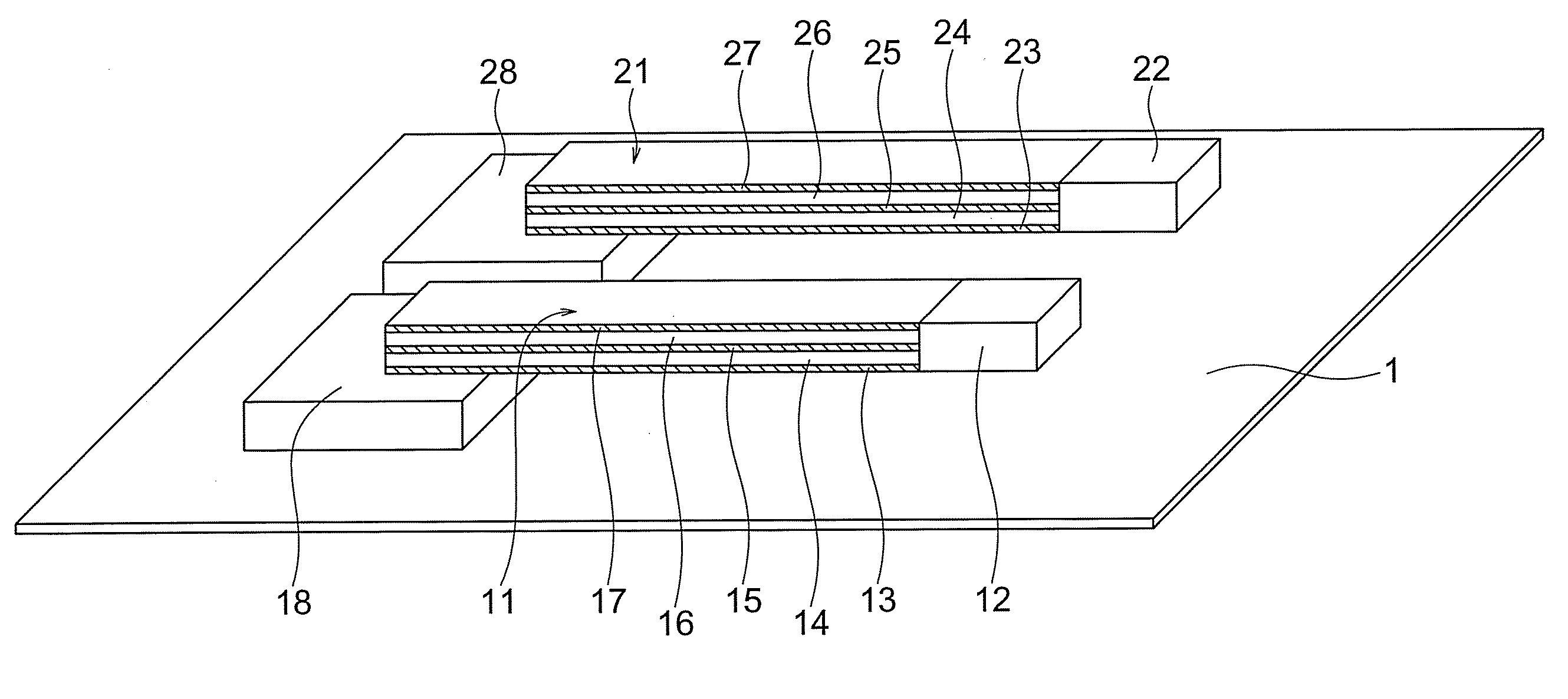
[0040]A piezoelectric driven MEMS device according to a first embodiment of the present invention is shown in FIG. 1. The piezoelectric driven MEMS device according to the present embodiment includes a first actuator 11 and a second actuator 21. A first end of the first actuator is a fixed end, and it is fixed to a substrate 1 through an anchor 18. The first actuator 11 includes a lower electrode 13, a piezoelectric film 14, an intermediate electrode 15, a piezoelectric film 16 and an upper electrode 17. The first actuator 11 is a piezoelectric driven actuator having the so-called bimorph structure. An action part 12 is connected to a second part of the first actuator 11.

[0041]The second actuator 21 is formed with the same stacked structure as that of the first actuator 11, under the same fabrication condition as that of the first actuator 11, or concurrently with the first actuator 11. A first end of the first actuator is a fixed end, and it is fixed to the substrate 1 through an a...

second embodiment

[0047]A piezoelectric driven MEMS device according to a second embodiment of the present invention is shown in FIG. 5. The piezoelectric driven MEMS device according to the present embodiment has a configuration in which the action part 12 in the first embodiment is formed of the lower electrode 13, the piezoelectric film 14, the intermediate electrode 15, the piezoelectric film 16 and the upper electrode 17 in the same way as the first actuator 11 and the action part 22 is formed of the lower electrode 23, the piezoelectric film 24, the intermediate electrode 25, the piezoelectric film 26 and the upper electrode 27 in the same way as the second actuator 21.

[0048]Fabricating the action parts 12 and 22 by using the materials used to form the actuators brings about an advantage that it becomes easy to hold down the displacements due to residual strains caused in the action parts, between the action parts and the actuators and the action parts can be formed simultaneously.

[0049]It is a...

third embodiment

[0052]A piezoelectric driven MEMS device according to a third embodiment of the present invention is shown in FIG. 6. The piezoelectric driven MEMS device according to the present embodiment has a configuration in which the action part 12 and the action part 22 in the first embodiment form a parallel plate capacitor to fabricate a variable capacitor.

[0053]The action part 12 is formed of the lower electrode 13 and the piezoelectric film 14, which are included in the first actuator 11. The action part 22 includes a main body part 22a, and an extension part 22b which is connected to the main body part 22a and which extends in a direction substantially perpendicular to the extension direction of the second actuator 21. In the same way as the second actuator 21, the main body part 22a includes the lower electrode 23, the piezoelectric film 24, the intermediate electrode 25, the piezoelectric film 26 and the upper electrode 27. The extension part 22b includes the intermediate electrode 25...


PUM


Abstract

A MEMS device includes: a first actuator having a first fixed end, including a stacked structure of a first lower electrode, a first piezoelectric film, and a first upper electrode, and being able to be operated by applying voltages to the first lower electrode and the first upper electrode; a second actuator having a second fixed end, being disposed in parallel with the first actuator, including a stacked structure of a second lower electrode, a second piezoelectric film, and a second upper electrode, and being able to be operated by applying voltages to the second lower electrode and the second upper electrode; and an electric circuit element having a first action part connected to the first actuator and a second action part connected to the second actuator.

Description

CROSS-REFERENCE TO RELATED APPLICATION[0001]This application is based upon and claims the benefit of priority from prior Japanese Patent Application No. 2006-98556 filed on Mar. 31, 2006 in Japan, the entire contents of which are incorporated herein by reference.BACKGROUND OF THE INVENTION[0002]1. Field of the Invention[0003]The present invention relates to a piezoelectric driven MEMS (Micro-electro-mechanical System) actuator.[0004]2. Related Art[0005]Recently, actuators fabricated by using the MEMS technique are drawing the attention. The actuators are driven by electrostatic force, thermal stress, electromagnetic force, piezoelectric force, and so on, and bent and displaced. An actuator using a piezoelectric thin film to rotate a shaft attached to a free end is known (see, for example, JP-A 2003-181800 (KOKAI)).[0006]Furthermore, MEMS devices such as variable capacitance type capacitors and switches using actuators are being studied. The variable capacitance type capacitors and s...

Claims


Application Information

Patent Timeline
IPC IPC(8): H01L41/00B81B3/00H01H57/00H01L41/09H02N2/00
CPCB81B3/0072B81B2201/032H01L41/094H01H57/00H01H2057/006H01G5/18H10N30/2042B81B3/00B81C1/00H10N30/20
Inventor NISHIGAKI, MICHIHIKONAGANO, TOSHIHIKOMIYAZAKI, TAKASHIITAYA, KAZUHIKOKAWAKUBO, TAKASHI
Owner KK TOSHIBA
Why Eureka
Try Eureka