Method for forming a patterned array of carbon nanotubes

a carbon nanotube and array technology, applied in the field of processing arrays of carbon nanotubes, can solve the problems of inability to employ expensive apparatuses, inability to effectively reduce or even eliminate the shielding effect, and inability to prevent the adjacent carbon nanotube from slipping, etc., to achieve the effect of simple manufacturing, cost-effectiveness and effective reduction or even elimination of the shielding

Active Publication Date: 2007-10-04
HON HAI PRECISION IND CO LTD +1
View PDF10 Cites 6 Cited by
  • Summary
  • Abstract
  • Description
  • Claims
  • Application Information

AI Technical Summary

Benefits of technology

[0009] Compared with conventional processing methods for arrays of carbon nanotubes, the preferred method of the present invention has the following advantages. The pattern of the carbon nanotubes is simple to manufacture and cost-effective. Because the top portion of the array of carbon nanotubes is divided into a plurality of separate units, the shielding effect can be effectively reduced or even eliminated. The field emission performance of the processed carbon nanotubes is improved.

Problems solved by technology

In a “raw” array, a shielding effect would unavoidably occur between adjacent carbon nanotubes.
If the synthesized array of carbon nanotubes is directly employed as an emitting structure in a field emission display, the field emission performance of the carbon nanotubes may be impaired.
However, the above-mentioned methods need to employ expensive apparatuses.
The cost of processing the arrays of carbon nanotubes via any of the above-mentioned methods is unduly high.
In addition, the apparatuses are relatively complicated to operate.

Method used


Image

  • Method for forming a patterned array of carbon nanotubes
  • Method for forming a patterned array of carbon nanotubes
  • Method for forming a patterned array of carbon nanotubes

Examples


Embodiment Construction

[0017] Reference will now be made to the drawings to describe preferred embodiments of the present invention in detail.

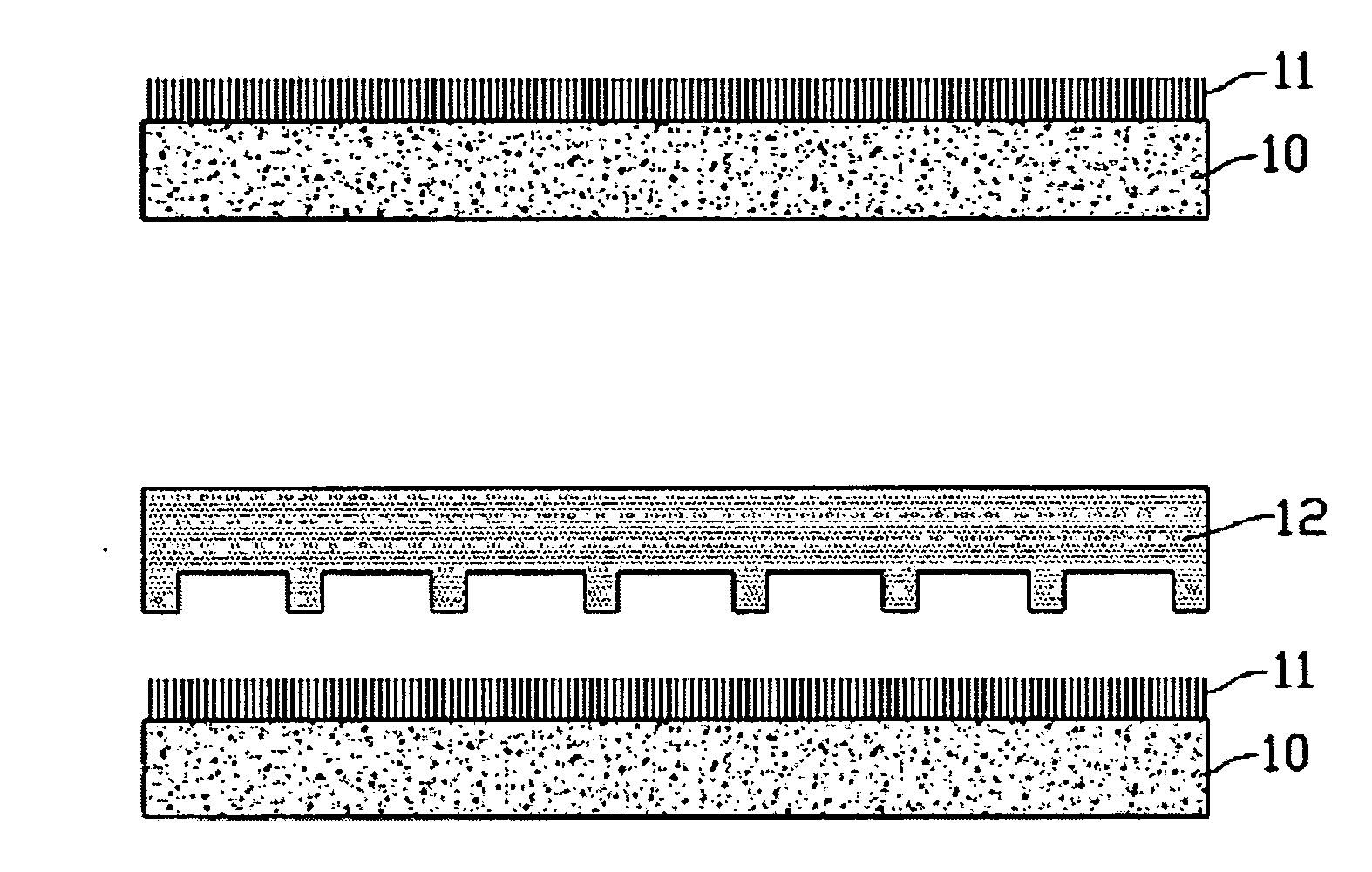
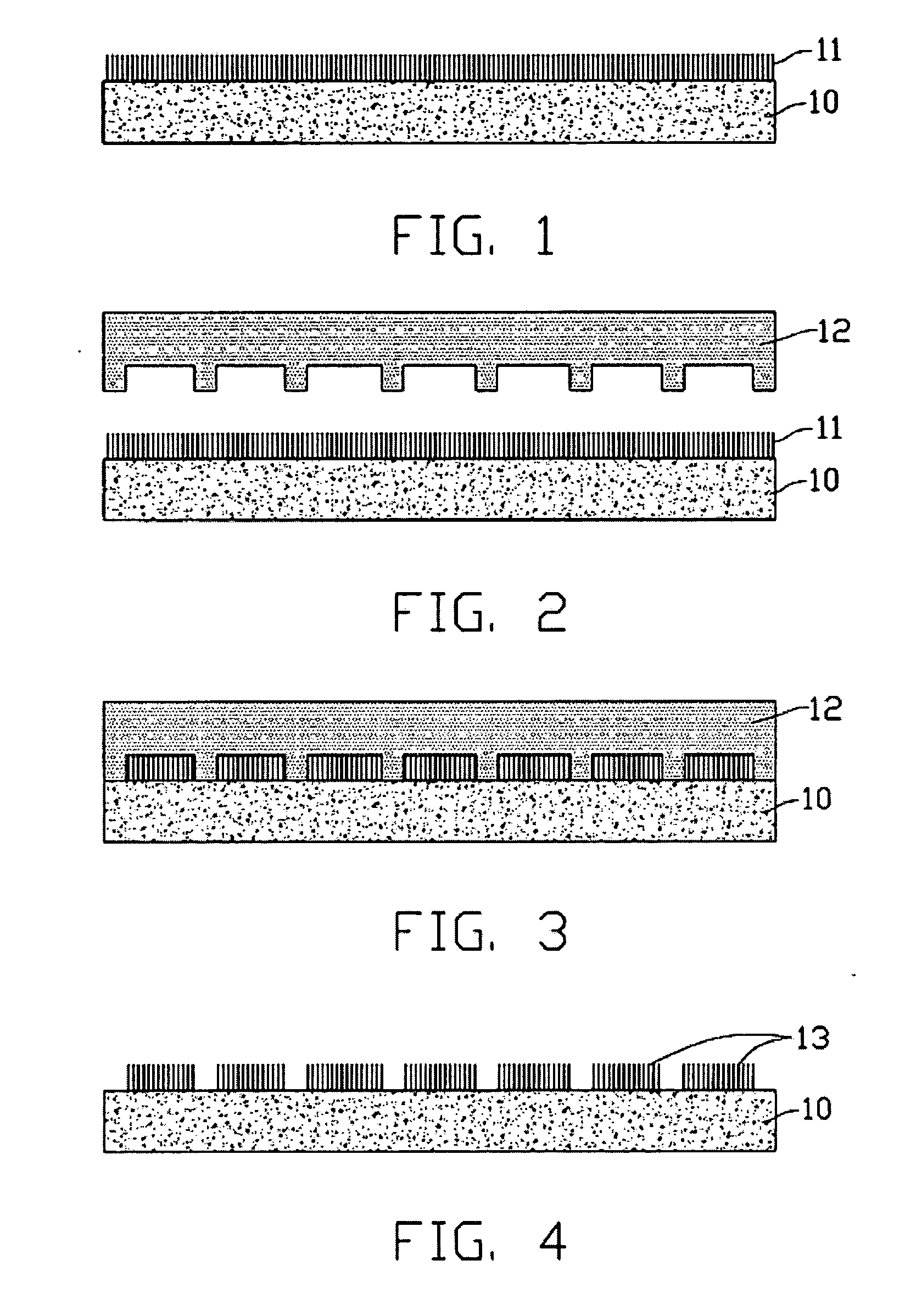
[0018] Referring to FIGS. 1 to 4, successive stages in a method for forming a patterned array of carbon nanotubes in accordance with a preferred embodiment of the present invention are shown. The method includes the steps of:

[0019] (a) providing a substrate 10, and forming an array of carbon nanotubes 11 on the substrate 10;

[0020] (b) providing a molding device 12 with a predetermined pattern, and imprinting the array of carbon nanotubes 11 with the molding device 12; and

[0021] (c) removing the molding device 12, thereby leaving the array of carbon nanotubes 13 having a pattern corresponding to the predetermined pattern of the molding device 12 defined therein.

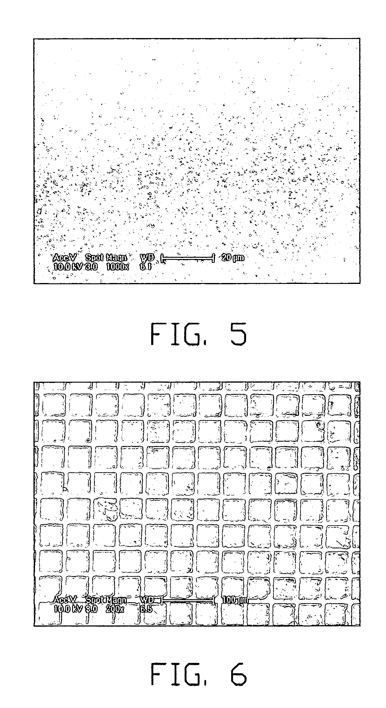
[0022] In step (a), the substrate 10 can be made of glass, silicon, metal, or a metal oxide. The array of carbon nanotubes 11 may be formed by a deposition method, or a printing method. The deposition met...


PUM

PropertyMeasurementUnit
threshold field emission voltageaaaaaaaaaa
current densityaaaaaaaaaa

Abstract

A method for forming a patterned array of carbon nanotubes (11) includes the steps of: forming an array of carbon nanotubes on a substrate (10); imprinting the array of carbon nanotubes using a molding device (12) with a predetermined pattern; and removing the molding device, thereby leaving a patterned array of carbon nanotubes (13). The method can effectively reduce or even eliminate any shielding effect between adjacent carbon nanotubes, and is simple to implement. The field emission performance of the patterned array of carbon nanotubes is improved.

Description

BACKGROUND OF THE INVENTION [0001] The present invention relates to methods for processing arrays of carbon nanotubes. [0002] Carbon nanotubes were first discovered by S. Iijima (Nature, vol. 354, pp. 56-58, 1991) and were synthesized by T. W. Ebbesen and P. M. Ajayan (Nature, vol. 358, pp. 220-222, 1992). Theoretical studies show that carbon nanotubes exhibit either metallic or semiconductive behavior depending on the radii and helicity of the nanotubes. Carbon nanotubes have interesting and potentially useful electrical and mechanical properties, and offer potential for use in electronic devices such as field emission displays, micro electron sources in vacuum, and nano-scale devices. However, to realize these various potential uses, specific methods for processing arrays of the carbon nanotubes may be necessary. [0003] For example, when arrays of carbon nanotubes are to be used in a field emission display, each array of carbon nanotubes must first be processed. This is because sy...

Claims


Application Information

Patent Timeline
Patent Type & Authority Applications(United States)
IPC IPC(8): B05D3/12C23C16/00
CPCB05D3/12B82Y10/00H01J2201/30469H01J9/025B82Y30/00
Inventor LIU, PENGSHENG, LEI-MEIWEI, YANGLIU, LIANGQIAN, LIHU, ZHAO-FUDU, BING-CHUCHEN, PI-JINFAN, SHOU-SHAN
Owner HON HAI PRECISION IND CO LTD
Why Eureka
Try Eureka