Method for forming metal bumps

a metal bump and metal technology, applied in the field of metal bump forming, can solve the problems of increasing cost, reducing product yield, and difficult to enhance the product yield of the package process, and achieve the effect of reducing time and cost of the package process, and solving the problem of poor uniform size of the metal bump

Inactive Publication Date: 2007-10-04
ADVANCED SEMICON ENG INC
View PDF17 Cites 23 Cited by
  • Summary
  • Abstract
  • Description
  • Claims
  • Application Information

AI Technical Summary

Benefits of technology

[0009]With the application of the aforementioned method for forming metal bumps, a planarization step is used to prevent the height of the metal layer formed by electroplating from being non-uniform, so the poor uniformity in sizes of the metal bumps can be solved. Therefore, compared to the conventional process, the method of the present invention is more suitable for a package process with fine pitch, and is more effective for reducing the time and cost of the package process.

Problems solved by technology

In the aforementioned prior art, the uniformity of the thickness of the metal layer 140 formed by plating is poor and the uniformity of the sizes of the metal bumps 150 is poor, so that the yield of the products is decreased in the package process.
In the current package process that require a fine pitch, the quality of the products manufactured by the prior art method cannot meet customer requirements and enhancing the product yield of the package process is difficult, thereby increasing the cost.

Method used


Image

  • Method for forming metal bumps
  • Method for forming metal bumps
  • Method for forming metal bumps

Examples


Embodiment Construction

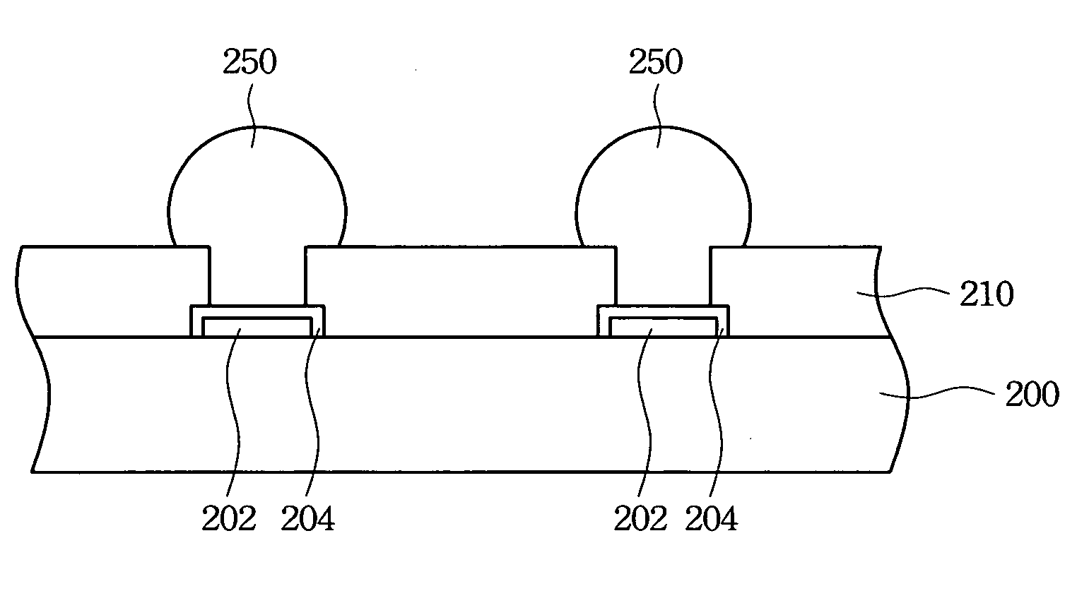
[0013]FIGS. 2A through 2E are schematic flow diagrams showing the process for manufacturing metal bumps in accordance with a preferred embodiment of the present invention. Firstly, such as shown in FIG. 2A, a substrate 200 is provided, wherein the substrate 200 includes a plurality of pads 202 formed thereon. In the embodiment, the substrate 200 is a printed circuit board, however, the other substrate including circuit set thereon may be used in the present invention, and the present invention is not limited thereto. In the embodiment, a protective layer 204 may be further formed on the pads 202 to increase the anti-oxidization of the pads 202, wherein a material of the protective layer 204 is selected from the group consisting of Au, Ni, Cu, Ag, Sn, Pb, Bi, Pd, Al, Fe, Cd, Zn and a combination thereof, or selected from organic solderability preservatives (OSP). Next, a patterned solder mask 210 is formed on the substrate 200, wherein the patterned solder mask 210 has a plurality of...


PUM

PropertyMeasurementUnit
conductiveaaaaaaaaaa
thicknessaaaaaaaaaa
heightaaaaaaaaaa

Abstract

A method for forming metal bumps is disclosed, comprising: providing a substrate including a plurality of pads; forming a solder mask on the substrate, wherein the solder mask has first openings to expose the pads; forming a photoresist layer on the solder mask, wherein the photoresist layer has second openings to expose the pads; forming a conductive layer on the phototresist layer, wherein a sidewall of each second opening, a sidewall of each first opening and the pads are covered with the conductive layer; forming a metal layer on the conductive layer by electroplating to fill the first and second openings; performing a planarization step to remove the conductive layer and the metal layer on the photoresist layer so as to remain the conductive layer and the metal layer in the first and second openings; removing the photoresist layer and performing a reflow step to form metal bumps.

Description

RELATED APPLICATIONS[0001]The present application is based on, and claims priority from, Taiwan Application Serial Number 95109039, filed Mar. 16, 2006, the disclosure of which is hereby incorporated by reference herein in its entirety.FIELD OF THE INVENTION[0002]The present invention relates to a method for forming metal bumps, and more particularly, to a method for forming metal bumps for a fine pitch package process.BACKGROUND OF THE INVENTION[0003]FIGS. 1A through 1E are schematic flow diagrams showing the conventional process for manufacturing metal bumps. As shown in FIG. 1A, a substrate 100 is initially provided, wherein the substrate 100 includes a plurality of pads 102 formed thereon. Next, a patterned solder mask 110 is formed on the substrate 100. In the method of forming the patterned solder mask 110, a solder mask 110 is deposed to cover the substrate 100, and a patterning step is performed to form a plurality of first openings 112 to expose the pads 102, wherein the pa...

Claims


Application Information

Patent Timeline
Patent Type & Authority Applications(United States)
IPC IPC(8): H01L21/44
CPCH01L21/4853H01L2924/01033H01L24/11H01L2224/0401H01L2224/114H01L2224/1147H01L2224/11474H01L2224/116H01L2224/13022H01L2224/13099H01L2924/01011H01L2924/01013H01L2924/01028H01L2924/01029H01L2924/0103H01L2924/01046H01L2924/01047H01L2924/0105H01L2924/01078H01L2924/01079H01L2924/01082H01L2924/014H05K3/243H05K3/3452H05K3/3473H05K2203/043H05K2203/054H05K2203/0588H01L2924/01019H01L24/03H01L2224/11502H01L2224/11849
Inventor WANG, SHENG-MINGCHANG, SHUO-HSUNCHANG, KUO-HUAHUANG, CHI-CHIHCHEN, CHIH-CHENG
Owner ADVANCED SEMICON ENG INC
Why Eureka
Try Eureka