Method and apparatus for plasma processing

a plasma processing and plasma technology, applied in the field of semiconductor semiconductor fabrication, can solve the problems of non-uniform electric field at the circumference, increase of fabrication cost, non-uniform wafer process, etc., and achieve the effect of maximizing the uniformity of process rate and processed structure shape, and significantly prolonging the life of the focus ring

Inactive Publication Date: 2007-10-04
NISHIO RYOJI +3
View PDF5 Cites 0 Cited by
  • Summary
  • Abstract
  • Description
  • Claims
  • Application Information

AI Technical Summary

Benefits of technology

[0038] As mentioned, according to the present invention, the focus ring structure can be optimized to correspond to the object of wafer processing through use of an equivalent circuit analysis, a two dimensional plasma analysis, a two dimensional electric field analysis and plasma-sheath interface flattening conditions, and through use of the optimized structure, can maximize the uniformity of the process rate and processed structure shape across the whole wafer surface.
[0039] Furthermore, the present invention enables to prevent deposition of process reaction products on the focus ring surface, by which the life of the focus ring can be extended significantly.

Problems solved by technology

However, a ceramic cover for protecting an electrostatic chuck is disposed near the outer circumference of the wafer, for example, which causes non-uniformity of the electric field at the circumference compared to the center of the wafer, and causes the drawback of non-uniformity of the wafer process.
These are serious problems since they cause the increase of fabrication costs
According to the above-mentioned prior art methods, however, there is no disclosure of a technique for optimizing the focus ring structure.
However, the prior art lacks to disclose such technique.
Therefore, the electric field correcting function of the focus ring changes with time and deteriorated.
Therefore, it is necessary to set up a tolerance and to optimize the structure accordingly, but the prior art lacks to disclose such technique.
The deposits on the focus ring surface may become particles that adhere to the wafer and cause defective products to be fabricated.
This may cause time variation of the wafer process according to which the result of wafer processing is changed with time from the starting of wafer processing.
The conventional methods lack to provide a method for coping with the deposition, so the focus ring may be helpful to uniformize the processing, but it is not actually useful if deposition occurs.
Of course, patent document 5 lacks to disclose any teachings related to determining the tolerance and optimizing the structure based thereon.
The drawback of the conventional optimization process disclosed in document 5 is that there is no teaching of a physical method or design technique for flattening the plasma-sheath interface above the wafer and the plasma-sheath interface above the focus ring.
The optimization of the structure is impossible to carry out without a physical mechanism or a design technique.
Even when an appropriate structure is discovered through experimental methods, it is difficult to prove experimentally that the plasma-sheath interface above the wafer and the plasma-sheath interface above the focus ring are flat, and the flatness cannot be ensured.
The drawback of the technique disclosed in patent document 6 mentioned above is that the generation of a uniform sheath voltage realized by equalizing the impedance between the lower electrode and plasma at the wafer portion and at the focus ring portion does not guarantee the flattening of the plasma-sheath interface above the wafer and the plasma-sheath interface above the focus ring.

Method used


Image

  • Method and apparatus for plasma processing
  • Method and apparatus for plasma processing
  • Method and apparatus for plasma processing

Examples


first embodiment

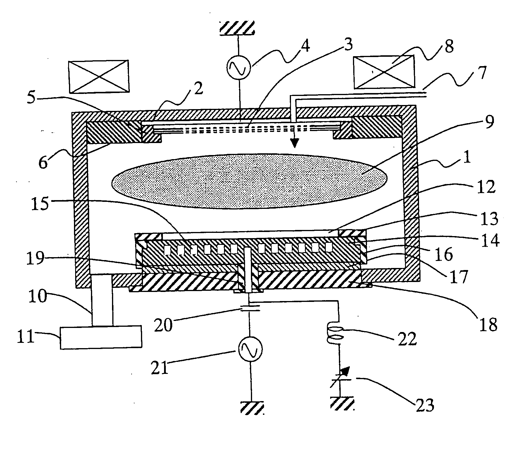
[0066] We will now describe the method of replacing the above-mentioned theory with a specific equivalent circuit model. For simplicity, a structure illustrated in FIG. 3 showing the present invention will be considered. On the surface of an electrode 33, a dielectric film 34 for electrostatic chucking is formed via thermal spray coating of alumina or the like. A wafer 30 and a focus ring 31 are mounted thereon, and a susceptor 32 for protecting the electrode 33 and dielectric film 34 is disposed. Although not shown, an RF power supply and a DC power supply for electrostatic chucking are connected to the electrode 33, by which the wafer 30 is chucked to the dielectric film 34, and the wafer 30 and focus ring 31 are subjected to RF bias.

[0067] Plasma region 37 is formed above the wafer 30 and focus ring 31, and an ion sheath region 36 is formed below a plasma-sheath interface 35. Now, the sheath thickness dsh given in formula 2 is the distance between the surface of wafer 30 (or focu...

second embodiment

[0087]FIG. 9 illustrates the present invention, in which a wafer 72 and a focus ring 73 are mounted on an electrode 70 having a dielectric film 71 for electrostatic chuck. A flat plasma-sheath interface 74 is formed above the wafer 72 and focus ring 73. The height of surfaces of the wafer 72 and the focus ring 73 are the same. In order to fulfill this condition, according to formula 8, HW=HFR and dW=dFR. In other words, V0−VW1=V0−VF1. From these equations, the following formula is obtained. [Formula⁢ ⁢9] ZW⁢ ⁢1ZW⁢ ⁢1+ZW⁢ ⁢2+ZW⁢ ⁢3=ZF⁢ ⁢1ZF⁢ ⁢1+ZF⁢ ⁢2+ZF⁢ ⁢3(9)

[0088] By forming simultaneous equations of formulas 7 and 9, the following formula 10 is obtained. This is the plasma-sheath interface flattening condition of FIG. 9.

[Formula 10]

ZW1:ZW2:ZW3=ZF1:ZF2:ZF3   (10)

[0089] By assigning individual conditions into formulas 7 and 8, the plasma-sheath interface flattening conditions corresponding to those specific conditions can be obtained. At this time, a gap (GWF) exists between th...

third embodiment

[0092] Regardless of the material of the focus ring, when a new focus ring is disposed, the thickness of the focus ring is determined so that the plasma-sheath interface above the focus ring is higher than the plasma-sheath interface above the wafer for a height corresponding to the tolerance of the sheath height difference, as illustrated in FIG. 11(a) showing the present invention. At this time, as shown in the circled portion of the drawing, the height difference of the plasma-sheath interface acts as a spherical lens for diverging ions with respect to the wafer. When the height of the plasma-sheath interface above the focus ring is reduced to the lowest tolerance from the plasma-sheath interface above the wafer due to consumption, the focus ring reaches its application limit, and will have to be replaced. At this time, as shown in the circled portion of the drawing, the height difference of the plasma-sheath interface acts as a spherical lens focusing the ions with respect to th...


PUM

PropertyMeasurementUnit
diameteraaaaaaaaaa
relative dielectric constantaaaaaaaaaa
capacitanceaaaaaaaaaa

Abstract

The invention provides a plasma processing apparatus capable of minimizing the non-uniformity of potential distribution around wafer circumference, and providing a uniform process across the wafer surface. The apparatus is equipped with a focus ring formed of a dielectric, a conductor or a semiconductor and having RF applied thereto, the design of which is optimized for processing based on a design technique clarifying physical conditions for flattening a sheath-plasma interface above a wafer and the sheath-plasma interface above the focus ring. A surface voltage of the focus ring is determined to be not less than a minimum voltage for preventing reaction products caused by wafer processing from depositing thereon. The surface height, surface voltage, material and structure of the focus ring are optimized so that the height of an ion sheath formed on the focus ring surface is either equal or has a height difference within an appropriate tolerance range to the height of the ion sheath formed on the wafer surface. Optimization of the structure is realized by setting up an appropriate tolerance range taking into consideration the variation caused by consumption of the focus ring.

Description

CROSS-REFERENCE TO RELATED APPLICATION [0001] This application is a Divisional application of application Ser. No. 10 / 902,032, filed Jul. 30, 2004, which claims priority from Japanese patent application No. JP 2004-118513, filed on Apr. 14, 2004, the contents of which are incorporated herein by reference in their entirety.FIELD OF THE INVENTION [0002] The present invention relates to the art of semiconductor fabrication. Especially, the invention relates to a structure of a wafer stage that affects the etching contour when providing an etching process to a semiconductor wafer using plasma. DESCRIPTION OF THE RELATED ART [0003] Recently, along with the enhancement in the integration of semiconductor elements, the circuit patterns have become more and more refined, and the demanded accuracy of processing dimension has become stricter. Further, the wafer diameter is increased to 300 mm in the attempt to reduce fabrication costs of the semiconductor elements, but processing is required ...

Claims


Application Information

Patent Timeline
Patent Type & Authority Applications(United States)
IPC IPC(8): H01L21/00H01L21/3065C23F1/00H01J37/32
CPCH01J37/32082H01J37/32642H01J37/32935G06F17/5081H01L21/6875G06F17/5086H01L21/67069G06F30/398G06F30/17
Inventor NISHIO, RYOJIKANEKIYO, TADAMITSUOOTA, YOSHIYUKIMATSUMOTO, TSUYOSHI
Owner NISHIO RYOJI
Why Eureka
Try Eureka