Multi-bit memory device and memory system

a memory device and multi-bit technology, applied in static storage, digital storage, instruments, etc., can solve problems such as data programming errors, charge leakage from floating gate, and reduced voltage margins between various threshold voltage distributions

Active Publication Date: 2007-10-04
SAMSUNG ELECTRONICS CO LTD
View PDF14 Cites 66 Cited by
  • Summary
  • Abstract
  • Description
  • Claims
  • Application Information

AI Technical Summary

Benefits of technology

[0022]In one embodiment, the invention provides a nonvolatile memory device comprising; a memory cell array comprising a plurality of memory blocks each having a plurality of memory cells adapted to store N bits, where N is an integer greater than 1, a page buffer configured to perform a read operation adapted to read data from the memory cell array and output read data, an error correction circuit configured to detect and correct an error in read data stored in a memory block K and generate corresponding error information, and a control circuit configured to reduce the number of bits stored in the plurality of memory cells for memory block K from N to J, where J is an integer less than N but greater than zero, in response to the error information.
[0023]In another embodiment, the invention provides a non-volatile memory system comprising; a memory controller configured to control read operations associated with a nonvolatile memory device, the nonvolatile memory device comprising, a memory cell array comprising a plurality of memory blocks each having a plurality of memory cells adapted to store N bits, where N is an integer greater than 1, wherein the memory cell array comprises a main data storage region adapted to store data and a spare data storage region adapted to store spare data associated with the data stored in the main storage region, and a page buffer configured to perform the read operation in relation to the memory cell array and output read data, the memory controller being configured to implement an error correction capability (ECC) adapted to detect and correct an error in the read data stored in a memory block K, and reduce the number of bits stored in the plurality of memory cells for memory block K from N to J, where J is an integer less than N but greater than zero, in response to the error detection.

Problems solved by technology

However, the use of an increased number of voltage distributions to indicate multi-bit data states necessarily reduces the voltage margins between the various threshold voltage distributions.
For example, if the insulation layer is thinner or thicker than designed, or if applied control voltages are too high or too low, data programming errors may occur.
Additionally, charge may leak from a floating gate over time.
Leaking charge may eventually result in a changed voltage distribution, and an erroneous data state.
Finally, the capability of flash memory cells to securely store charge tends to diminish over time (i.e., after being programmed and read many times).
However, since highly energetic charge injection and emission mechanisms are used to repeatedly manipulate the charge state on the floating gate, insulation defects and charge traps are often formed within the insulation layer surrounding the floating gate (e.g., the tunnel oxide).
The development of such defects and traps creates reliability problems most commonly manifest during write and erase operations applied to the memory cell.
The uncontrolled and undesired loss (leakage) or accumulation of charge on a floating gate inevitably results in an increased or decreased threshold voltage for the EEPROM memory cell.
Such threshold voltage deviations result in randomly occurring data bit errors.
Error(s) in the read data may in many instances be due to degradations resulting from repeated programming and erasure operations applied to the nonvolatile memory device.
In terms of general error generation characteristics, the possibility of repeated error generation is very high for a memory block in the memory cell array having previously detected errors.
Such errors result in reduced reliability of conventional multi-bit nonvolatile memory devices and the designation of many bad blocks.
However, the designation of multiple bad blocks leads to reducing overall data storage capacity.

Method used


Image

  • Multi-bit memory device and memory system
  • Multi-bit memory device and memory system
  • Multi-bit memory device and memory system

Examples


Embodiment Construction

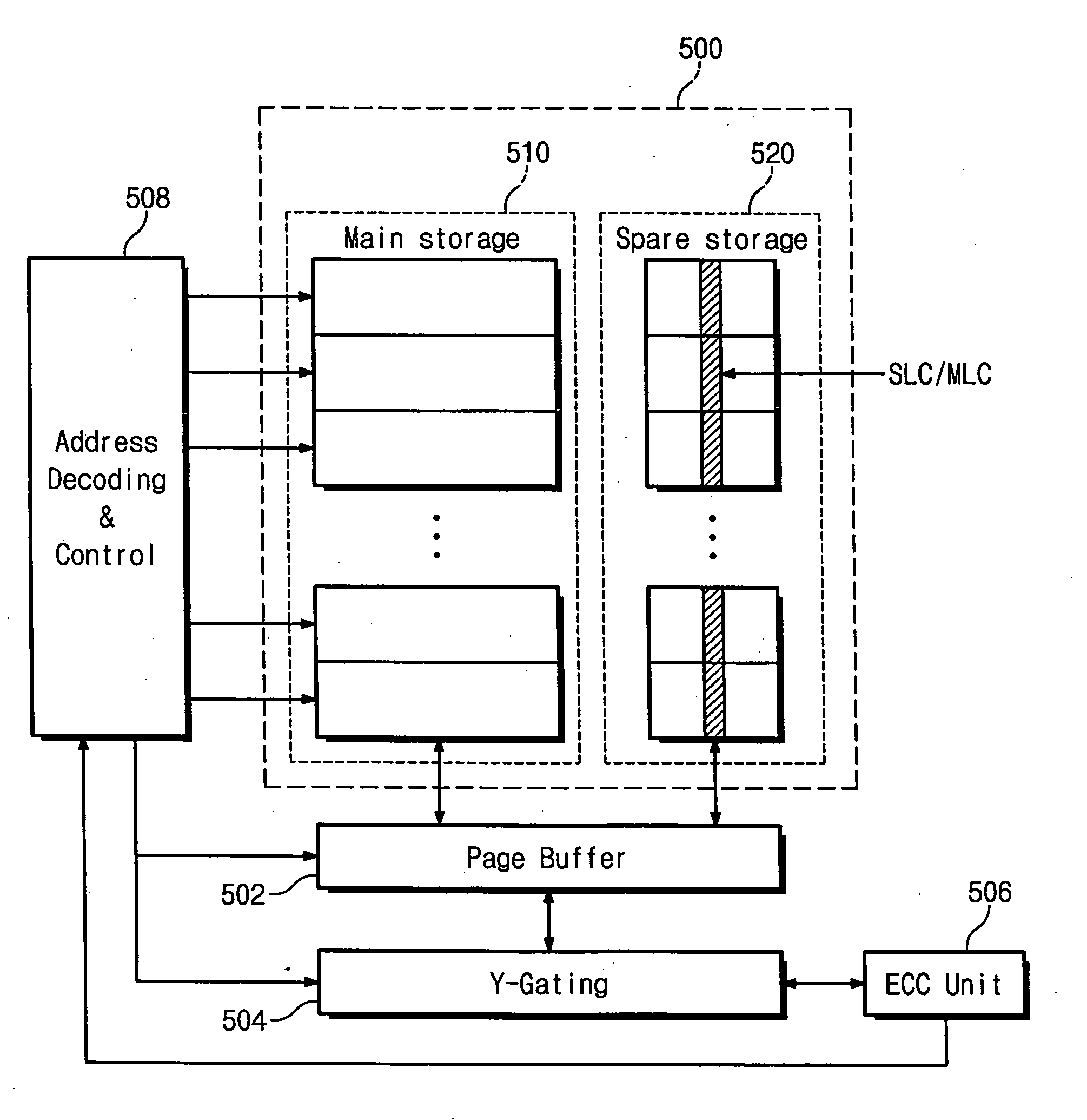
[0034]Embodiments of the invention will now be described in some additional detail with reference to the accompanying drawings. However, the invention may be embodied in many different forms and should not be construed as being limited to only the embodiments set forth herein. Rather, the illustrated embodiments are presented as teaching examples. Throughout the specification and drawings, like reference numbers refer to like or similar elements.

[0035]FIG. 5 is a block diagram of a nonvolatile memory including an error correction circuit (ECC) according to an embodiment of the invention. The nonvolatile memory includes a memory cell array 500, a page buffer 502, an error correction circuit (ECC) 506, an address decoding and control circuit 508, and a column gating circuit 504. Memory cell array 500 includes a plurality of memory blocks each having a plurality of nonvolatile memory cells. Page buffer 502 latches write data to be written into memory cell array 500 and read data read f...


PUM


Abstract

A nonvolatile memory device, memory system and read method are disclosed. The memory device comprises a memory cell array comprising a plurality of memory blocks each having a plurality of memory cells adapted to store N bits, where N is an integer greater than 1, a page buffer configured to perform a read operation adapted to read data from the memory cell array and output read data, an error correction circuit configured to detect and correct an error in read data stored in a memory block K and generate corresponding error information, and a control circuit configured to reduce the number of bits stored in the plurality of memory cells for memory block K from N to J, where J is an integer less than N but greater than zero, in response to the error information.

Description

BACKGROUND OF THE INVENTION[0001]1. Field of the Invention[0002]The present invention relates to a nonvolatile memory device and memory system incorporating same. More specifically, the present invention is directed to electrically programmable / erasable nonvolatile memory cells and related memory systems.[0003]This non-provisional patent application claims priority under 35 U.S.C § 119 to Korean Patent Application 2006-29691 filed on Mar. 31, 2006, the entirety of which is hereby incorporated by reference.[0004]2. Description of Related Art[0005]Due to their ease of use, electrically programmable / erasable nonvolatile memories such as flash memory are rapidly replacing other types of nonvolatile memory, such as erasable programmable read only memories (EPROMs) or mask read only memories (mask ROMs), in the design of many contemporary host devices. For example, flash memory is now commonly used to store programming code.[0006]Indeed, with advances in related semiconductor fabrication ...

Claims


Application Information

Patent Timeline
Patent Type & Authority Applications(United States)
IPC IPC(8): G11C29/00
CPCG11C11/5628G11C11/5642G11C16/04G11C16/0483G11C29/00G11C2211/5642G11C29/44G11C29/52G11C2029/0409G11C2211/5641G11C29/42G11C16/22
Inventor HWANG, SANG-WONLEE, JONG-SOO
Owner SAMSUNG ELECTRONICS CO LTD
Why Eureka
Try Eureka