Plurality of capacitors employing holding layer patterns and method of fabricating the same

a layer pattern and capacitor technology, applied in the field of semiconductor substrates, can solve the problems of 2-bit failure and low plate drop, and achieve the effects of preventing the leaning increasing the height of the lower plate, and sufficient capacitan

Inactive Publication Date: 2007-10-11
AHN TAE HYUK
View PDF34 Cites 12 Cited by
  • Summary
  • Abstract
  • Description
  • Claims
  • Application Information

AI Technical Summary

Benefits of technology

[0012] A further object of the present invention is to provide a method of fabricating a plurality of capacitors having sufficient capacitance by increasing the height of lower plates, while preventing leaning of the lower plates during the fabrication process.
[0013] In accordance with an exemplary embodiment, the present invention provides a plurality of capacitors employing holding layer patterns. The plurality of capacitors includes a plurality of cylinder-shaped lower plates repeatedly aligned on a same plane in two dimensions. Holding layer patterns are located between uppermost portions and lowermost portions of the plurality of lower plates, and connect the adjacent side walls of the plurality of lower plates. An upper plate fills the spaces inside the plurality of lower plates and the spaces between the side walls thereof. A capacitor dielectric layer is interposed between the plurality of lower plates and the upper plate, and insulates the lower plates and the upper plate. As such, the holding layer patterns are located between the side walls of the lower plates to support the lower plates. As a result, the structure serves to avoid leaning of the lower plates.
[0019] In accordance with an exemplary embodiment, the present invention provides a semiconductor device having a plurality of capacitors employing holding layer patterns. The semiconductor device includes a semiconductor substrate. A plurality of cylinder-shaped lower plates are aligned repeatedly over the semiconductor substrate in two dimensions. Holding layer patterns are located between uppermost portions and lowermost portions of the plurality of lower plates, and connect the adjacent side walls of the plurality of lower plates. An upper plate fills the spaces inside the plurality of lower plates and the spaces between the side walls thereof. A capacitor dielectric layer is interposed between the plurality of lower plates and the upper plate, and insulates the lower plates and the upper plate.
[0021] In accordance with a further exemplary embodiment, the present invention provides a method of fabricating a plurality of capacitors employing holding layer patterns. The method includes preparing a semiconductor substrate having a lower insulating layer. A plurality of storage contact plugs repeatedly aligned in two dimensions are formed inside the lower insulating layer. An etch barrier layer and a lower sacrificial oxide layer are sequentially formed on the semiconductor substrate having the storage contact plugs. A holding layer having openings exposing the lower sacrificial oxide layer is formed on the lower sacrificial oxide layer. Herein, the centers of the respective openings are located above portions of the lower insulating layer that are surrounded by the storage contact plugs. An upper sacrificial oxide layer is formed over the semiconductor substrate having the holding layer with the openings. The upper sacrificial oxide layer, the holding layer, the lower sacrificial oxide layer, and the etch barrier layer are sequentially patterned using photolithography and etch processes, to form capacitor holes exposing the storage contact plugs and holding layer patterns. The holding layer patterns are exposed inside the capacitor holes. Then, lower plates covering the inner walls of the capacitor holes are formed, and the upper sacrificial oxide layer and the lower sacrificial oxide layer between the lower plates are sequentially removed. As the holding layer patterns support the lower plates, even though the upper sacrificial oxide layer and the lower sacrificial oxide layer between the lower plates are removed, falling-down of the lower plates can be avoided.
[0025] In accordance with another exemplary embodiment, the present invention provides a method of fabricating a plurality of capacitors employing holding layer patterns. The method includes preparing a semiconductor substrate having a lower insulating layer. A plurality of storage contact plugs repeatedly aligned in two dimensions are formed inside the lower insulating layer. An etch barrier layer and a lower sacrificial oxide layer are sequentially formed on the semiconductor substrate having the storage contact plugs, and the lower sacrificial oxide layer is partially etched to form grooves repeatedly aligned in two dimensions. Herein, the centers of the respective grooves are located above portions of the lower insulating layer that are surrounded by the storage contact plugs. Then, spacers covering the inner walls of the grooves are formed. An upper sacrificial oxide layer is formed on the semiconductor substrate having the spacers. The upper sacrificial oxide layer, the spacers, the lower sacrificial oxide layer, and the etch barrier layer are sequentially patterned using photolithography and etch processes, to form capacitor holes exposing the storage contact plugs and holding layer patterns. Herein, the holding layer patterns are exposed inside the capacitor holes. Then, lower plates covering the inner walls of the capacitor holes are formed, and the upper sacrificial oxide layer and the lower sacrificial oxide layer between the lower plates are sequentially removed. As the holding layer patterns are formed of spacers having a wide lower side and a narrow upper side, it is easy to form a following capacitor dielectric layer and an upper plate between the lower plates. Thus, the height of the holding layer patterns can be increased.

Problems solved by technology

However, with the increase of height of the lower plates, there often occurs a phenomenon that the lower plates fall down, and lean toward other adjacent lower plates.
The phenomenon, which is called “leaning”, results in the lower plates being electrically connected, and causes a 2-bit failure.

Method used


Image

  • Plurality of capacitors employing holding layer patterns and method of fabricating the same
  • Plurality of capacitors employing holding layer patterns and method of fabricating the same
  • Plurality of capacitors employing holding layer patterns and method of fabricating the same

Examples


Embodiment Construction

[0036] The present invention will now be described more fully hereinafter with reference to the accompanying drawings, in which preferred embodiments of the invention are shown. This invention may, however, be embodied in different forms and should not be construed as limited to the embodiments set forth herein. Rather, these embodiments are provided so that this disclosure will be thorough and complete, and will fully convey the scope of the invention to those skilled in the art. In the drawings, the thickness of layers and regions are exaggerated for clarity. Like numbers refer to like elements throughout the specification.

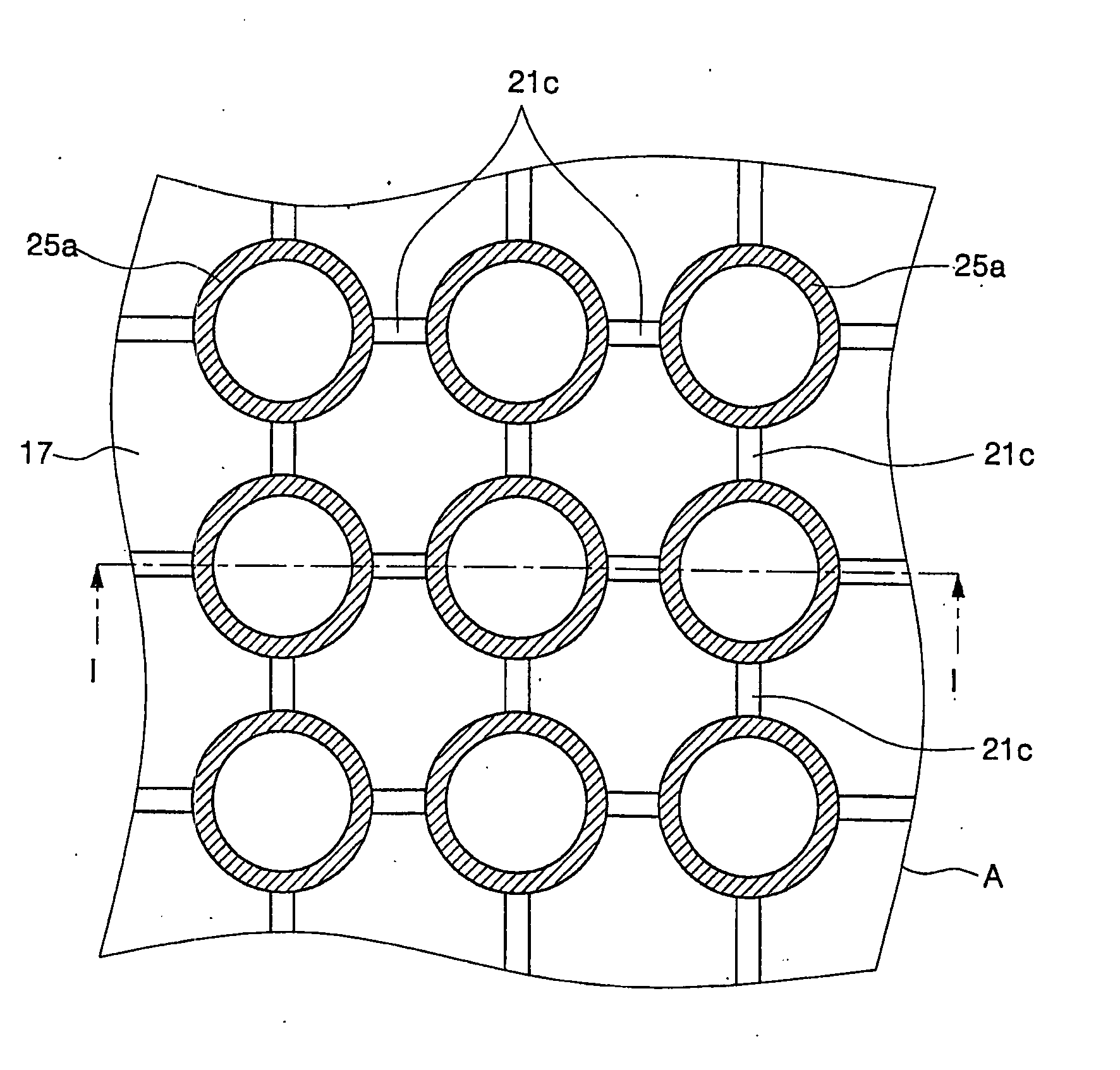
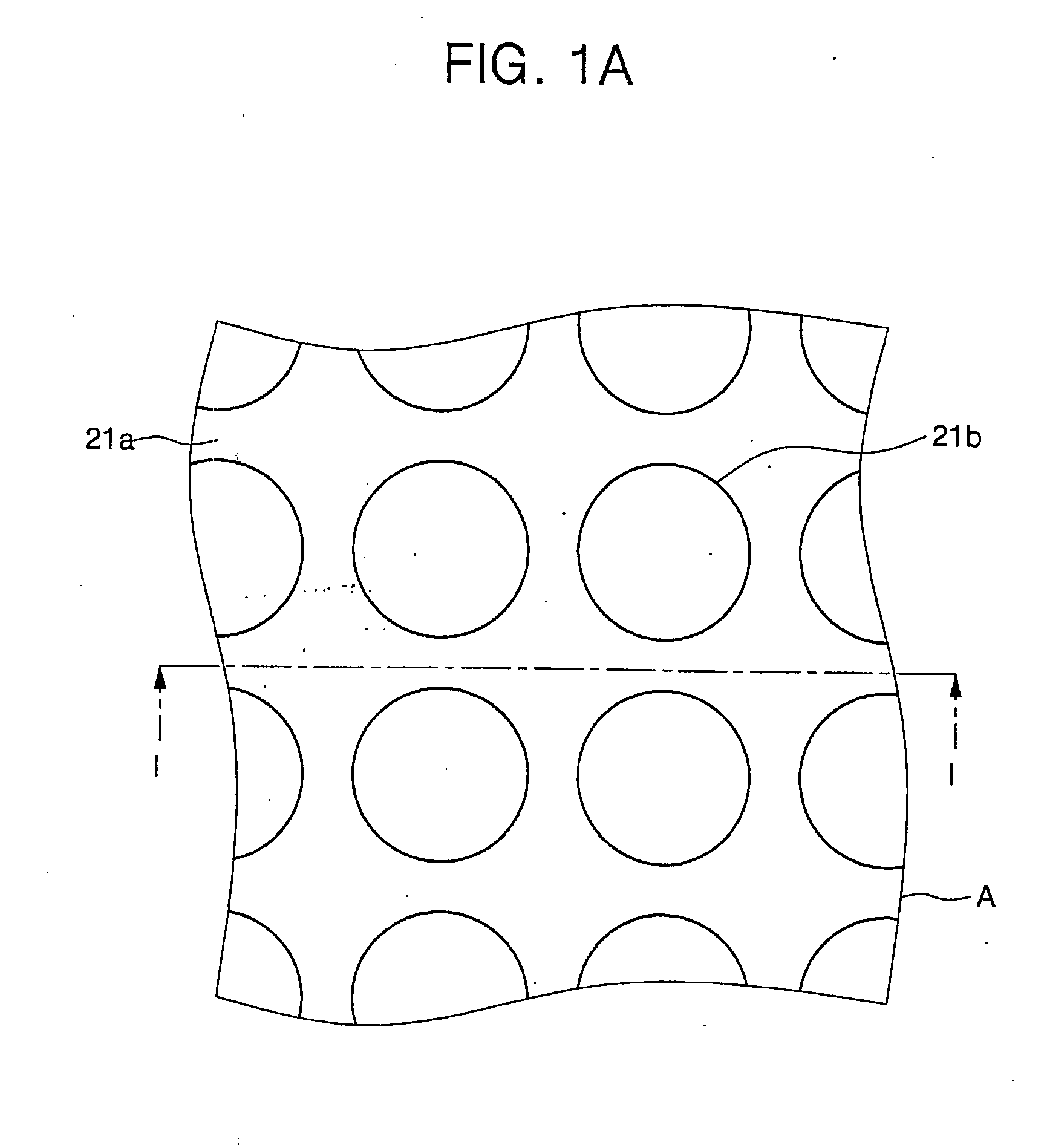
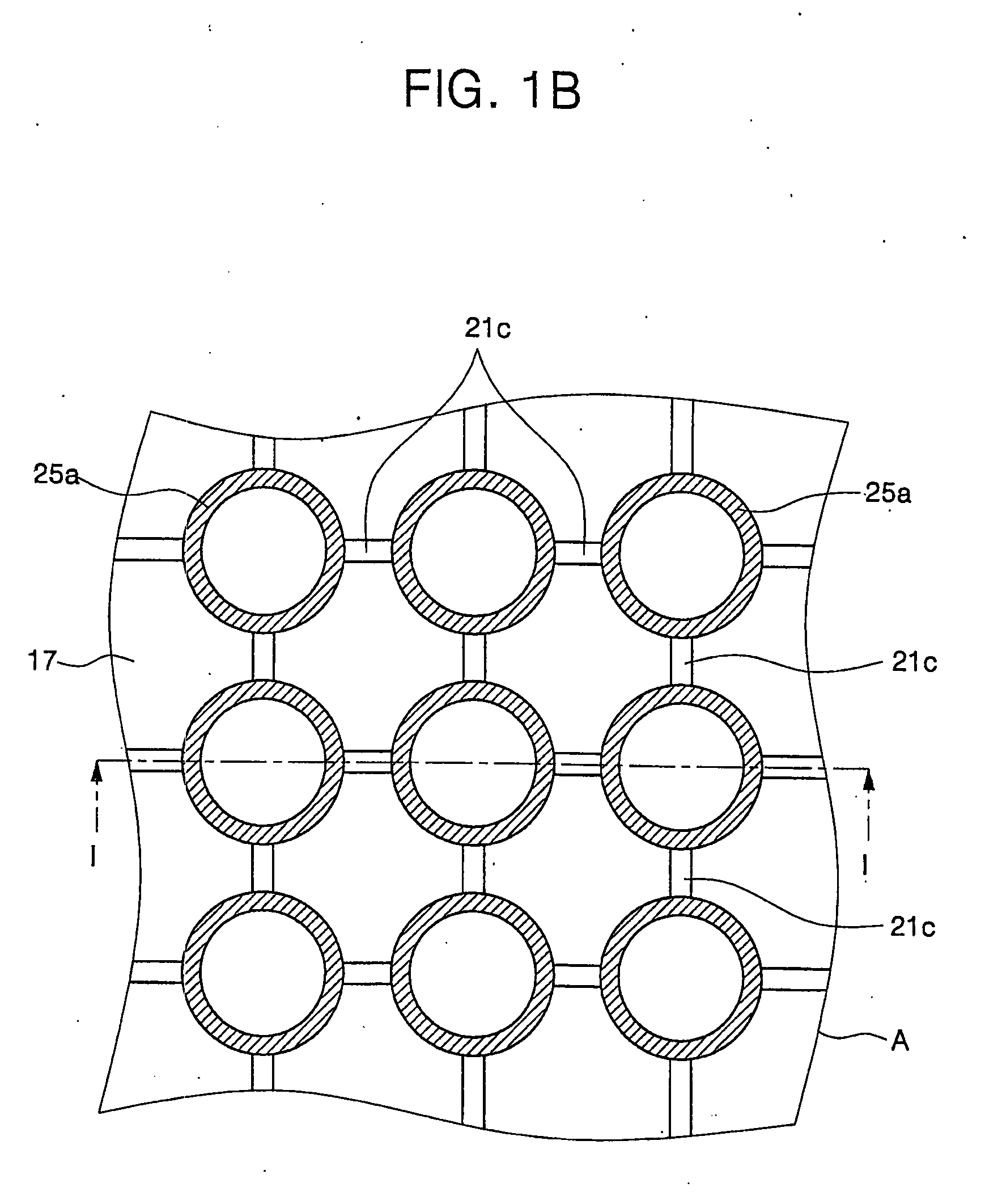
[0037]FIGS. 1A and 1B are top plan views respectively showing a holding layer having openings, and a plurality of lower plates to illustrate a method of fabricating a plurality of capacitors according to one embodiment of the present invention. FIGS. 2A to 2I are sectional views illustrating a method of fabricating a plurality of capacitors according to one emb...


PUM

PropertyMeasurementUnit
etch rateaaaaaaaaaa
thicknessaaaaaaaaaa
non-conductiveaaaaaaaaaa

Abstract

A plurality of capacitors employing holding layer patterns, and a method of fabricating the same, the plurality of capacitors including a plurality of cylinder-shaped lower plates repeatedly aligned in two dimensions. Holding layer patterns are located between the uppermost portions and the lowermost portions of the plurality of lower plates, and connect the adjacent side walls of the plurality of lower plates. An upper plate fills the spaces inside the plurality of lower plates and the spaces between the side walls of the plurality of lower plates. A capacitor dielectric layer is interposed between the plurality of lower plates and the upper plate, and insulates the lower plates and the upper plate.

Description

CROSS-REFERENCE TO RELATED APPLICATIONS [0001] This is a divisional of application Ser. No. 09 / 971,022, filed Oct. 25, 2004, which is incorporated herein by reference in its entirety. [0002] A claim of priority is made to Korean Patent Application No. 2003-77414, filed on Nov. 3, 2003, the disclosure of which is hereby incorporated herein by reference in its entirety.BACKGROUND OF THE INVENTION [0003] 1. Field of the Invention [0004] The present invention relates to a semiconductor substrate and a method of fabricating the same, and more particularly, to a plurality of capacitors employing holding layer patterns and a method of fabricating the same. [0005] 2. Description of the Related Art [0006] Memory devices such as DRAM require a plurality of cell capacitors having sufficient capacitance in order to improve resistance to a particles and increase a refresh cycle. In order to realize a capacitor having sufficient capacitance, it is necessary to increase an overlap space between an...

Claims


Application Information

Patent Timeline
Patent Type & Authority Applications(United States)
IPC IPC(8): H05K3/00H04R17/00H01L21/02H01L21/8242H01L27/02H01L27/108
CPCH01L27/0207H01L27/10814H01L27/10852Y10T29/42Y10T29/49117Y10T29/49124Y10T29/435H01L28/91H10B12/315H10B12/033H10B99/00
Inventor AHN, TAE-HYUK
Owner AHN TAE HYUK
Why Eureka
Try Eureka