Solar Cell Module and Manufacturing Process Thereof

a solar cell module and manufacturing process technology, applied in the field can solve the problems of reducing the yield in the manufacturing process of solar cell modules, cracks in semiconductor substrates,

Inactive Publication Date: 2007-10-11
KYOCERA CORP
View PDF8 Cites 181 Cited by
  • Summary
  • Abstract
  • Description
  • Claims
  • Application Information

AI Technical Summary

Benefits of technology

[0038] These and other advantages, features and effects of the invention will become apparent from the following description of specific embodiments with reference to the accompanying drawings.

Problems solved by technology

This stress may cause cracks to occur in the semiconductor substrate 101.
In addition, the solar cell element 104 may break or have significant cracks during the subsequent laminate process where the solar cell element 104 is encapsulated with a filler, which causes yield in the manufacturing process of solar cell module to drop.

Method used


Image

  • Solar Cell Module and Manufacturing Process Thereof
  • Solar Cell Module and Manufacturing Process Thereof
  • Solar Cell Module and Manufacturing Process Thereof

Examples


example 1

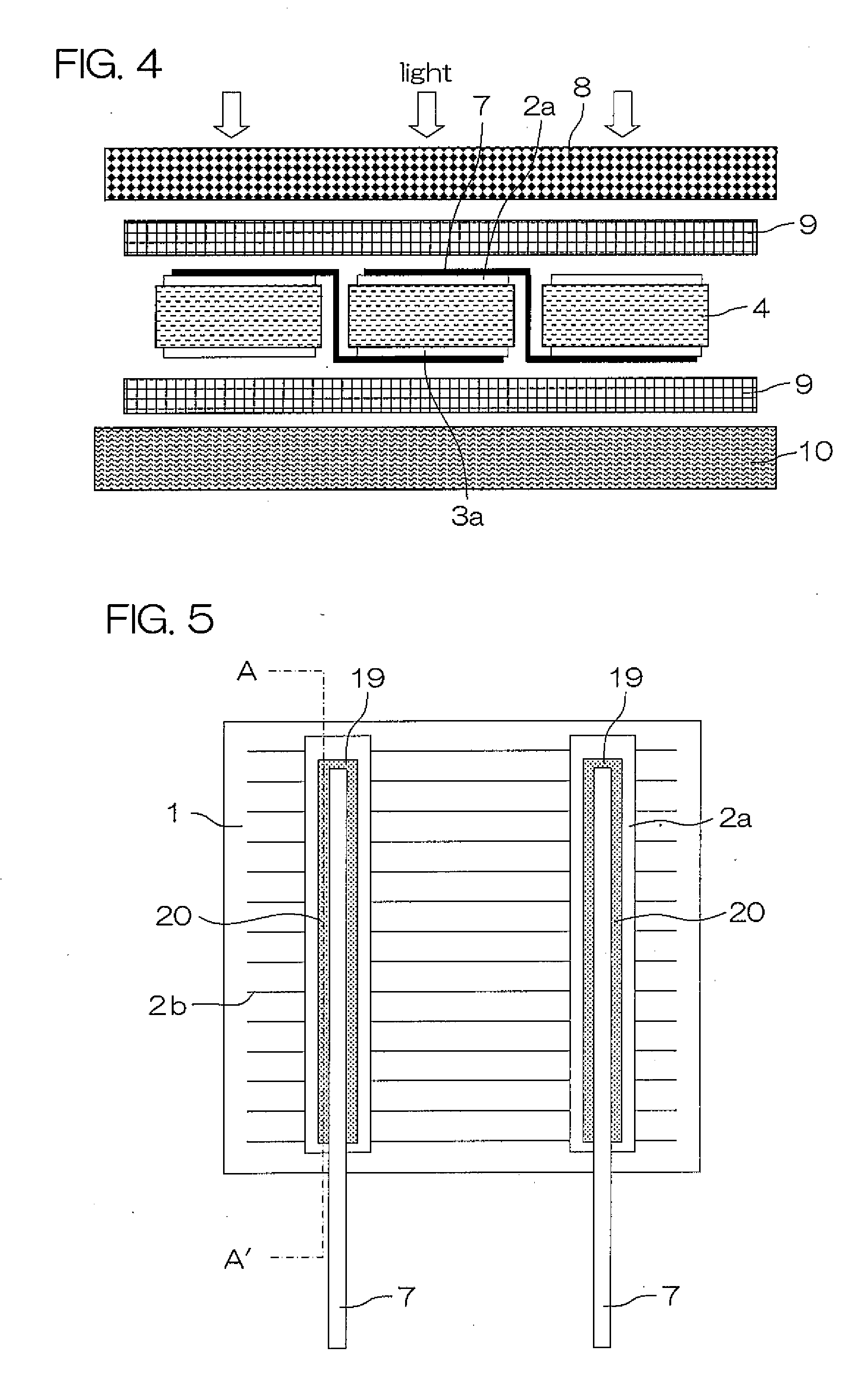
[0148] Solar cell modules were fabricated with the shapes of the fillet 19 shown in FIGS. 8 and 9 by changing some of height A of the fillet 19, indentation amount −L and bulge amount L. The height A of the fillet 19 was generally the same as the height H of the connection tab 7. Ten samples were prepared for each of L / A and −L / A, and the strengths of stress applied to the substrate 1 after welding the connection tab 7 were calculated.

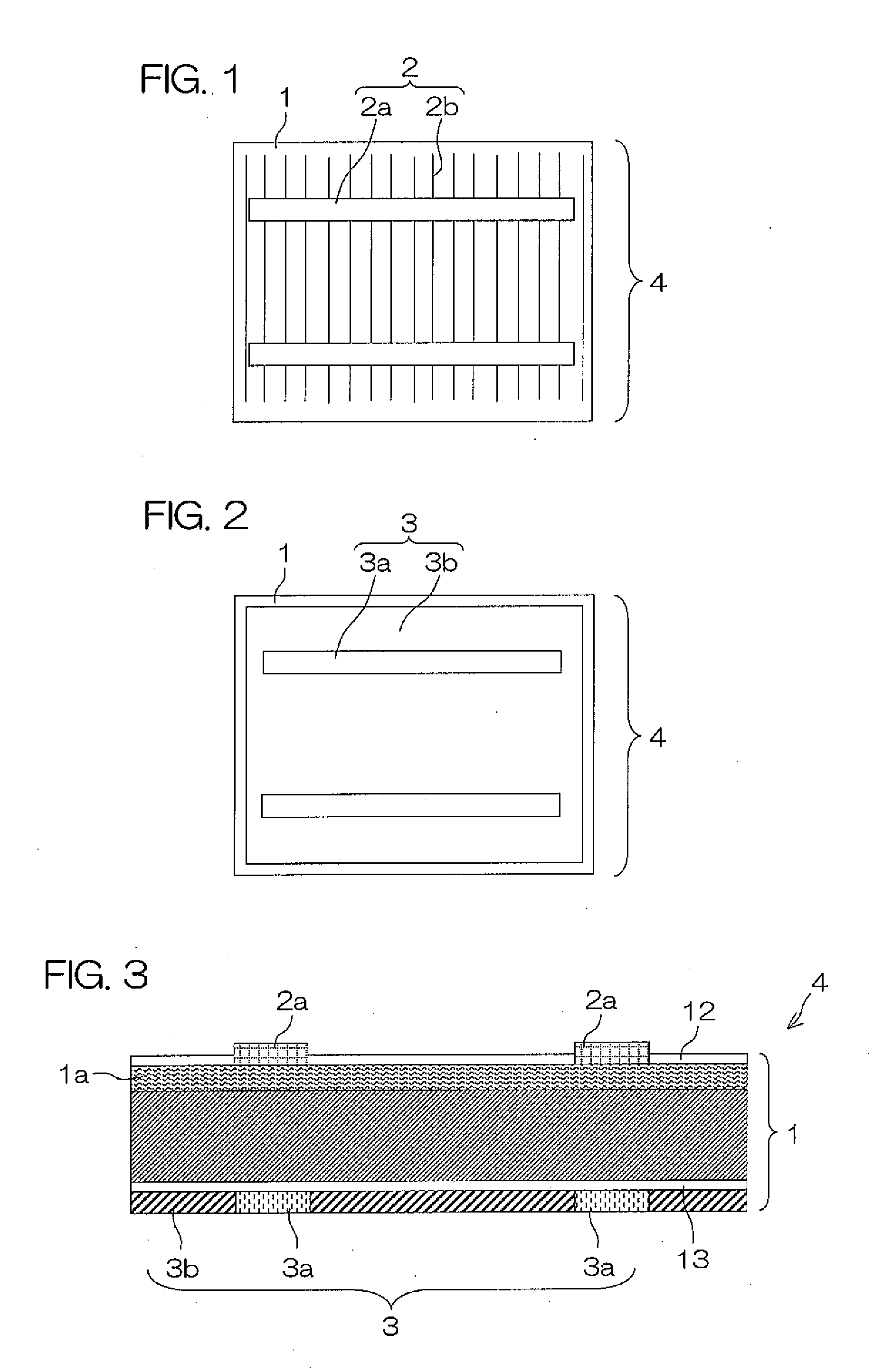
[0149] The samples were prepared in the following way. A damaged layer on the surface of a semiconductor element 1 comprising p-type multicrystalline silicon that has a thickness of 100 μm and outer dimensions of 15 cm by 15.5 cm was etched with NaOH to be cleaned. Then, this semiconductor element 1 was placed in a diffusion furnace to be heated in phosphorous oxychloride (POCl3) so that phosphorus atoms were diffused in the surface of the semiconductor element 1 to form an n-type region. In addition, a silicon nitride film with a thickness of 850 Å w...

example 2

[0165] An organic electrode material including silver powder was used as the bonding material for welding the connection tab 7 to the light receiving surface bus bar electrode 2a or non-light receiving surface bus bar electrode 3a.

[0166] Meanwhile, the “organic electrode material including silver powder” refers to an electrode material in the form of paste composed mainly of silver powder, in which an organic vehicle and glass frit were added, the amounts of which were 10-30 parts by weight and 0.1-5 parts by weight, respectively, with respect to 100 parts by weight of silver. In welding the connection tab 7, a solder in a molten state was supplied to an end portion of the connection tab 7 on the bus bar electrode 2a, 3a, thereby forming a fillet 19. When the shape of the fillet 19 satisfied −0.54≦L / A≦0.1, stress Fx and stress Fy do not exceed the threshold value, and it is expected that no cracking occurs.


PUM

PropertyMeasurementUnit
widthaaaaaaaaaa
temperatureaaaaaaaaaa
thicknessaaaaaaaaaa

Abstract

In a solar cell module, a solder fillet 19 is formed on an end surface on the shorter length side of a connection tab to be connected to a bus bar electrode 2a, 3a up to the height of the connection tab. The geometry of the solder fillet 19 is adjusted so that an indentation amount is 0-54% of the height or a bulge amount is 0-10% of the height, by which the maximum principal stress generated during the manufacturing process of a solar cell element 4 can be reduced, and therefore occurrences of cracks can be reduced. Also during a laminating process, breaking of the solar cell element or crack generation can be eliminated.

Description

BACKGROUND OF THE INVENTION [0001] 1. Field of the Invention [0002] The present invention relates to a solar cell module including a plurality of solar cell elements connected to each other by means of connection tabs and a manufacturing process thereof, and in particular, to a solar cell module and a manufacturing process thereof in which yield in the manufacturing process is improved. [0003] 2. Description of Related Art [0004] With the increasing attention to global environment issues and energy saving measures in recent years, new energy technologies utilizing natural energy have been receiving attention. As one of such technologies, systems utilizing solar energy are attracting a high level of interest, and in particular, spread of household use of photovoltaic power generation systems has been accelerated. [0005] A solar cell element is fabricated using monocrystalline silicon or multicrystalline silicon with thickness of about 0.3-0.4 mm and size of about 150 mm square. This ...

Claims


Application Information

Patent Timeline
Patent Type & Authority Applications(United States)
IPC IPC(8): H01L31/00
CPCB32B17/10018B32B17/10761H01L31/1876Y02E10/50H01L31/0504B32B17/10788Y02P70/50
Inventor NAGATA, MASARUKIYOHARA, TOSHIFUMINISHI, KOUJI
Owner KYOCERA CORP
Why Eureka
Try Eureka