

Method for conditioning a process chamber
a technology of process chamber and control method, which is applied in the direction of chemistry apparatus and processes, cleaning of hollow objects, coatings, etc., can solve the problems of deterioration of process characteristics, change process, and inability to simply refer to the process data displayed, so as to achieve the characteristic deterioration of the process, the ability to detect early stage abnormalities and process changes
- Summary
- Abstract
- Description
- Claims
- Application Information
AI Technical Summary
Problems solved by technology
Method used
Image

Examples
Embodiment Construction
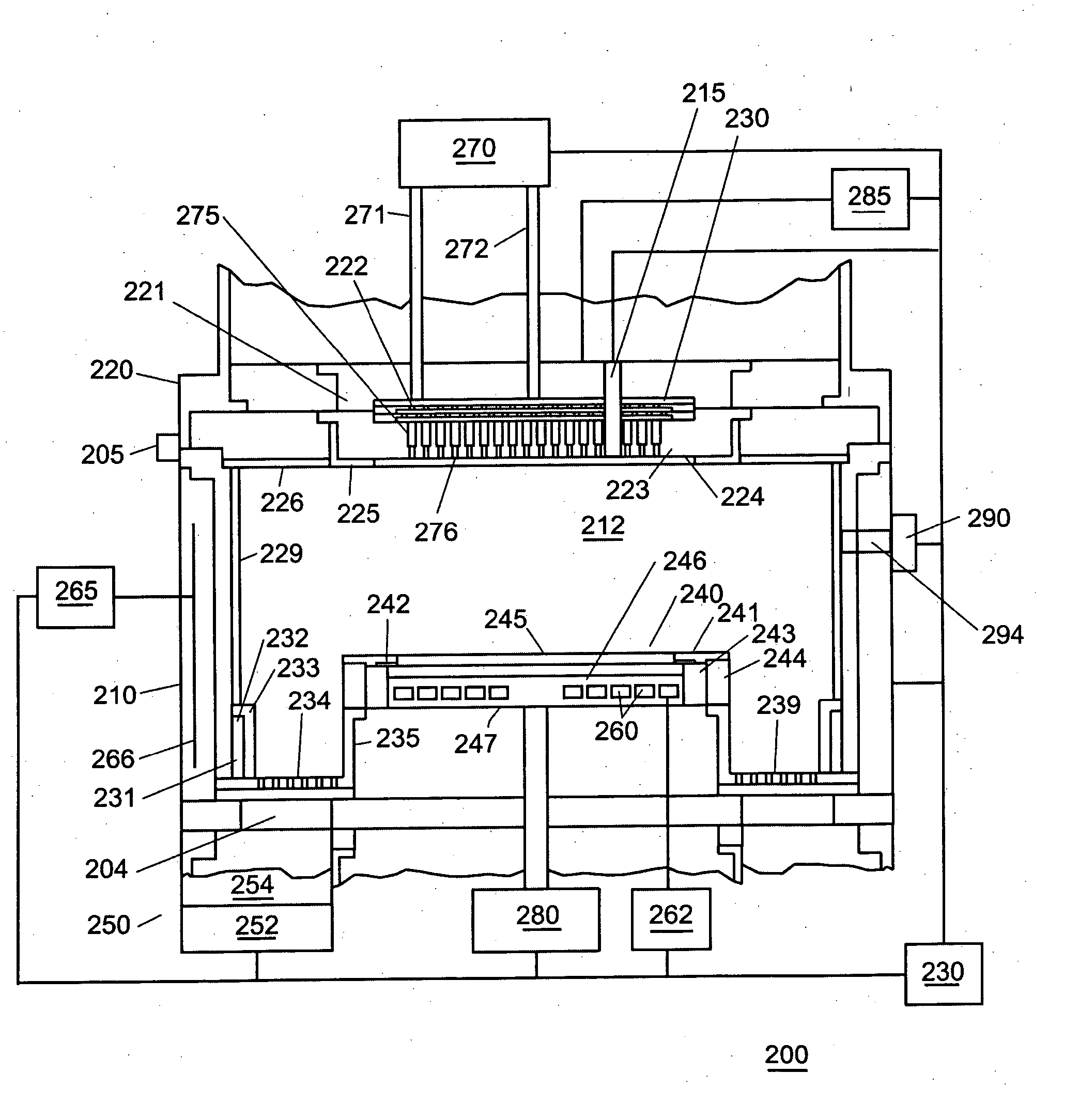
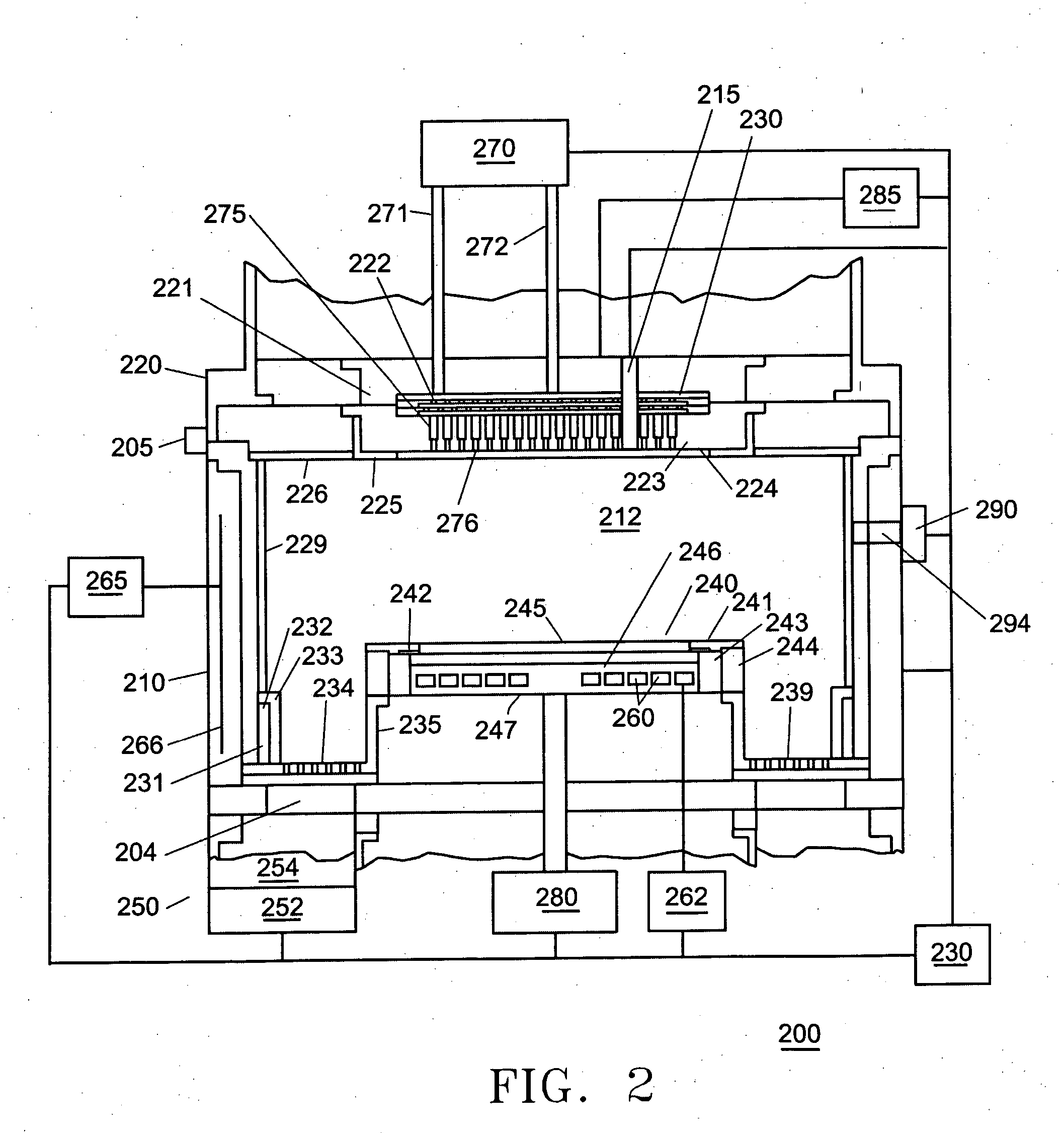
[0011] The present invention provides a method and apparatus for controlling process parameters at the wafer-to-wafer level. By using closely integrated measurement devices, it is possible to provide real time measurements of the critical dimensions (CD) of the incoming material. For example, the process recipe can include a target CD indicating the desired critical dimension after the process is completed. The purpose of the run-to-run (R2R) controller is to provide a set of recipe parameters for each wafer that will achieve the desired results using wafer-to-wafer (W2W) control.
[0012] The relationship between the desired process results and the process parameters needed to achieve those results is called the process model. For example, in an etch tool, there can be a simple relationship between the amount of material that needs to be etched, the etch rate and the etch time.
[0013] The performance of any process tool is expected to drift over time, and the process model can includ...
PUM
| Property | Measurement | Unit |
|---|---|---|
| pressure | aaaaa | aaaaa |
| pressure | aaaaa | aaaaa |
| RF power | aaaaa | aaaaa |
Abstract
Description
Claims
Application Information