Manufacturing method of semiconductor device

a manufacturing method and semiconductor technology, applied in semiconductor devices, semiconductor/solid-state device details, electrical devices, etc., can solve the problems of reducing the reliability of the semiconductor device thus manufactured, affecting and reducing the production yield, so as to achieve the effect of improving the reliability of the semiconductor devi

Active Publication Date: 2008-03-25
RENESAS ELECTRONICS CORP
View PDF8 Cites 40 Cited by
  • Summary
  • Abstract
  • Description
  • Claims
  • Application Information

AI Technical Summary

Benefits of technology

[0006]Generation of a tensile stress in the channel region of an n channel MISFET is effective for improving the source•drain current of the n channel MISFET. The tensile stress can be generated in the channel region of an n channel MISFET by forming a silicon nitride film for self aligned contact process over a semiconductor substrate by using low-pressure CVD so as to cover a gate electrode.
[0007]The present inventors have found that, when, for the purpose of reducing the contact resistance, a cobalt silicide layer is formed over a gate electrode and a semiconductor region serving as a source•drain by the Salicide (Self Aligned Silicide) process and, then, a silicon nitride film for self aligned contact process is formed over the semiconductor substrate, including the upper surface of the cobalt silicide layer, by low-pressure CVD, there is a possibility that the silicon nitride film will exhibit an abnormal growth. If an abnormal growth of the silicon nitride film occurs, an abnormal growth portion of the silicon nitride film remains on the bottom of a contact hole upon formation thereof in an interlayer insulating film, and it increases the contact resistance between the plug formed in the contact hole and the gate electrode or semiconductor region serving as a source•drain, which may lead to a conduction failure therebetween. This lowers the reliability of the semiconductor device thus manufactured and reduces the production yield.
[0008]An object of the present invention is to provide a technology capable of improving the reliability of a semiconductor device.
[0016]The reliability of a semiconductor device can be improved by the present invention.

Problems solved by technology

If an abnormal growth of the silicon nitride film occurs, an abnormal growth portion of the silicon nitride film remains on the bottom of a contact hole upon formation thereof in an interlayer insulating film, and it increases the contact resistance between the plug formed in the contact hole and the gate electrode or semiconductor region serving as a source•drain, which may lead to a conduction failure therebetween.
This lowers the reliability of the semiconductor device thus manufactured and reduces the production yield.

Method used


Image

  • Manufacturing method of semiconductor device
  • Manufacturing method of semiconductor device
  • Manufacturing method of semiconductor device

Examples


embodiment 1

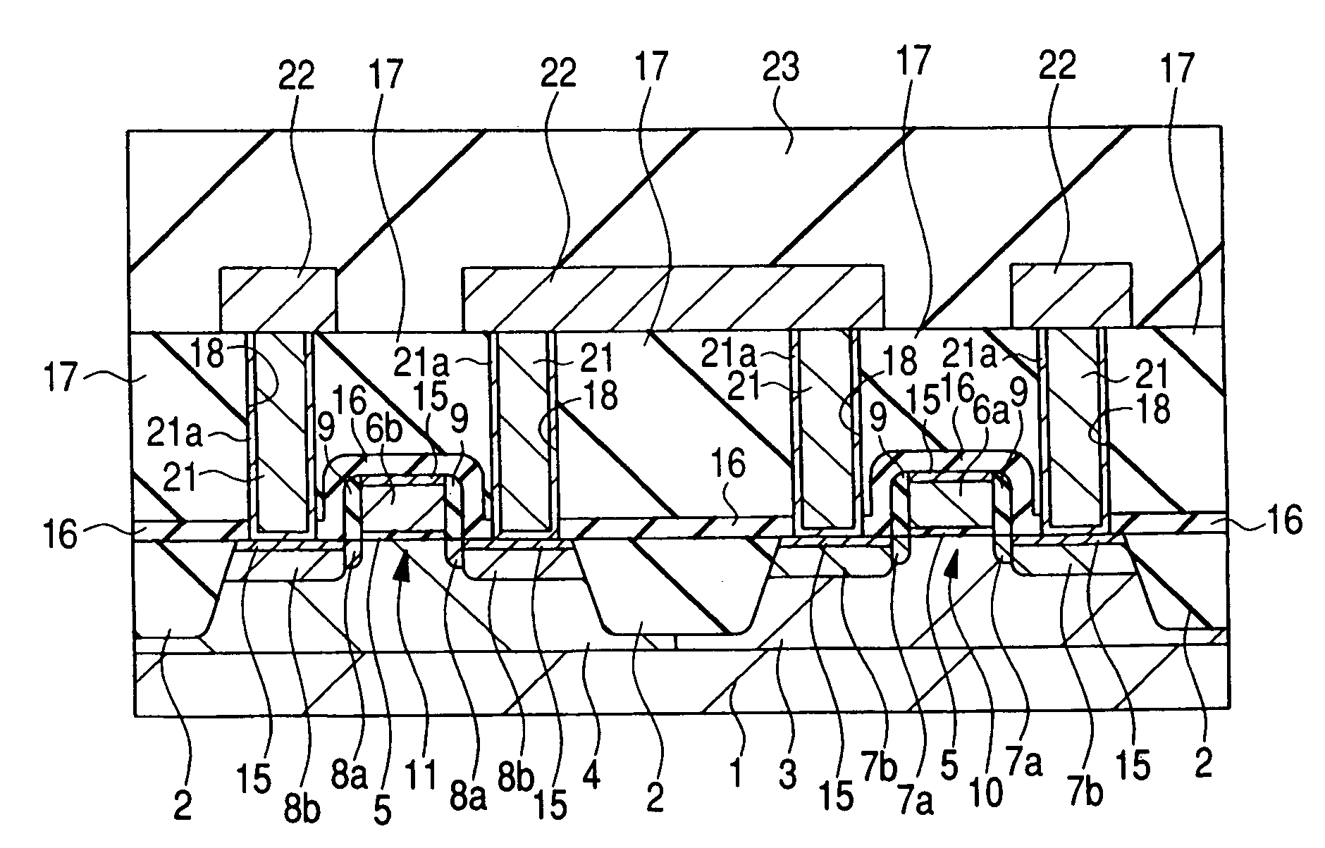
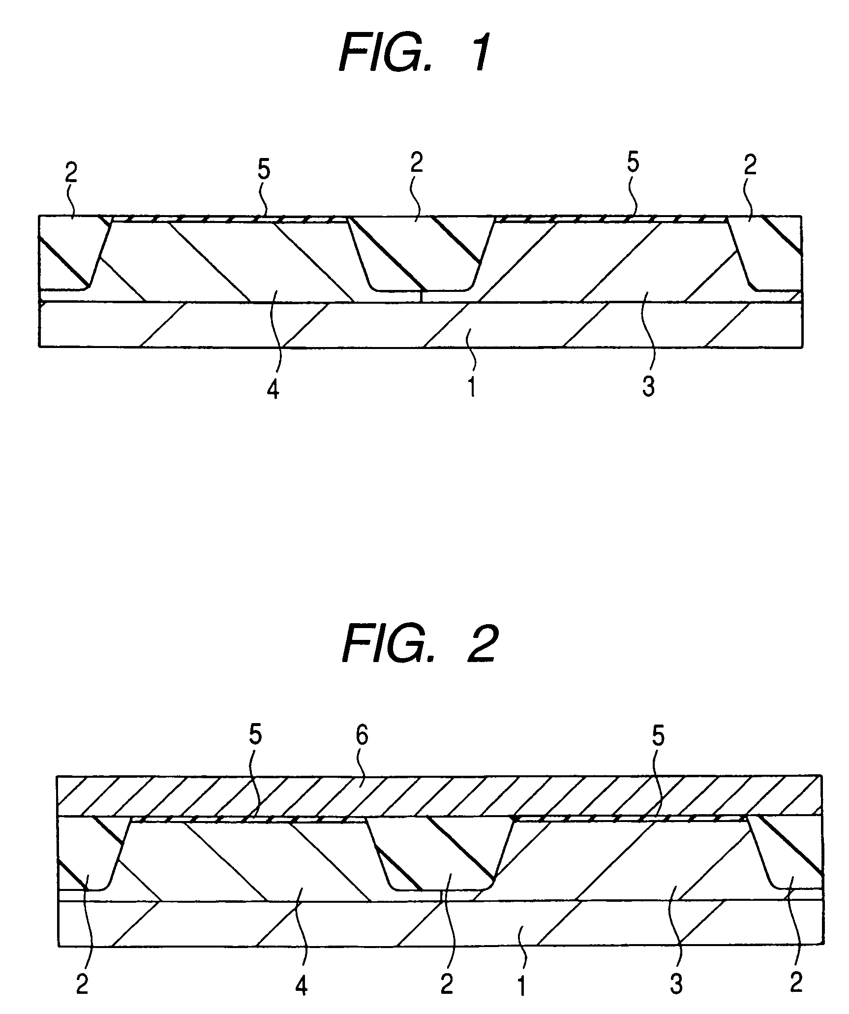
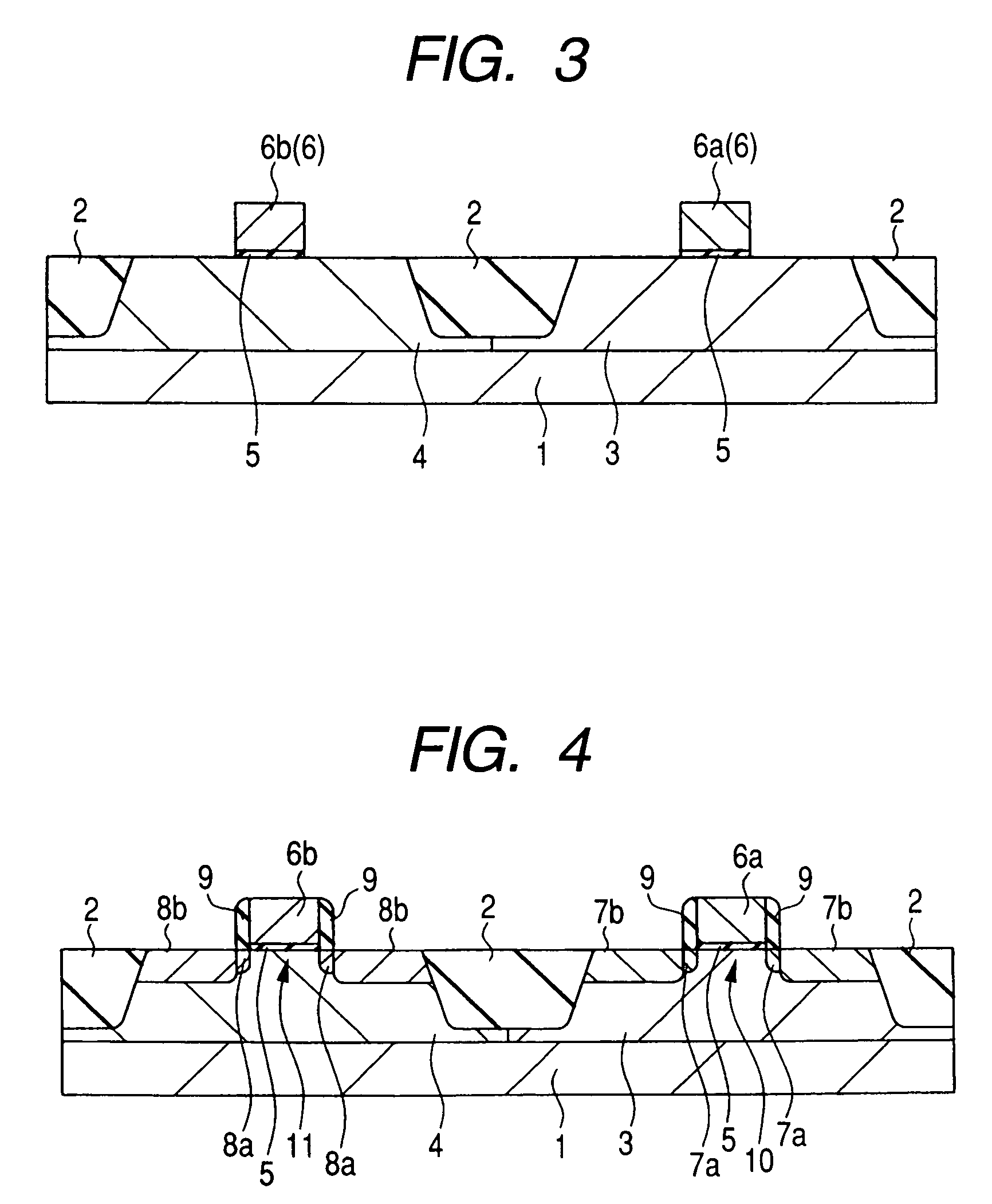
[0045]A semiconductor device according to this Embodiment and the manufacturing steps thereof will be described with reference to the accompanying drawings. FIG. 1 is a fragmentary cross-sectional view of a semiconductor device, for example, a CMISFET (Complementary Metal Insulator Semiconductor Field Effect Transistor), according to one embodiment of the invention, as seen during a manufacturing step.

[0046]As illustrated in FIG. 1, a semiconductor substrate (semiconductor wafer) 1, which is made of, for example, a p type single crystal silicon having a specific resistance of from 1 to 10 Ωcm, is prepared. Over the main surface of the semiconductor substrate 1, an element isolation region 2 is formed. The element isolation 2 is made of silicon oxide and it can be formed, for example, by STI (Shallow Trench Isolation) or LOCOS (Local Oxidization of Silicon).

[0047]A p-well 3 and an n-well 4 are each formed in the semiconductor substrate 1 to a predetermined depth from the main surface...

embodiment 2

[0086]FIG. 22 is a flow chart of a manufacturing process showing steps in the manufacture of a semiconductor device according to another embodiment of the invention. The manufacturing process is substantially similar to that of Embodiment 1 until the second annealing (second heat treatment) of Step S4. A description of the manufacturing steps prior to the second annealing of Step S4 is therefore omitted, and those steps performed thereafter will be described next.

[0087]In this Embodiment, the second wet cleaning of Step S5 of Embodiment 1 is replaced with plasma treatment using ammonia (NH3). After the second annealing of Step S4 similar to Embodiment 1, plasma treatment is performed (Step S5a) in this Embodiment. Plasma treatment using ammonia (NH3) is preferred. Nuclei 31 as described above can be chemically or physically removed from the surface of the CoSi2 layer 15 by this plasma treatment (ammonia plasma treatment).

[0088]After the plasma treatment of Step S5a, a silicon nitrid...

embodiment 3

[0092]FIG. 23 is a flow chart of a manufacturing process showing steps in the manufacture of a semiconductor device according to a further embodiment of the invention. The manufacturing process is substantially similar to that of Embodiment 1 until the second annealing (second heat treatment) of Step S4. A description of the manufacturing steps up to the second annealing of Step S4 is therefore omitted, and those steps provided thereafter will be described next.

[0093]In this Embodiment, the second wet cleaning of Step S5 according to Embodiment 1 is replaced by sputter etching (sputter etch). More specifically, after the second annealing of Step S4 similar to that of Embodiment 1, sputter etching is performed by using, for example, argon (Ar) (Step S5b) in this Embodiment. Nuclei 31 as described above on the surface of the CoSi2 layer 15 can be removed physically by this sputter etching. The nuclei 31 exist more in the vicinity of the surface of the CoSi2 layer 15 than inside of the...


PUM

PropertyMeasurementUnit
temperatureaaaaaaaaaa
thicknessaaaaaaaaaa
thicknessaaaaaaaaaa

Abstract

A method of manufacture of a semiconductor device includes forming a gate insulating film and a gate electrode made of polycrystalline silicon over a semiconductor substrate; implanting ions into the semiconductor substrate to form a semiconductor region as a source or drain; forming a cobalt film and a titanium nitride film over the semiconductor substrate to cover the gate electrode; carrying out annealing to cause a reaction between Co and Si and the semiconductor region to form a CoSi layer; carrying out wet cleaning to remove the titanium nitride film and unreacted cobalt film to leave the CoSi layer over the gate electrode and semiconductor region; carrying out annealing to cause a reaction between the CoSi layer and the gate electrode and semiconductor region to form a CoSi2 layer; carrying out HPM cleaning; and forming over the semiconductor substrate a silicon nitride film by low-pressure CVD to cover the gate electrode.

Description

CROSS-REFERENCE TO RELATED APPLICATION[0001]The present application claims priority from Japanese patent application No. 2003-411509, filed on Dec. 10, 2003, the content of which is hereby incorporated by reference into this application.BACKGROUND OF THE INVENTION[0002]The present invention relates in general to a method of manufacture of a semiconductor device and to a semiconductor device, more particularly, the invention relates to a technique that is effective when applied to the manufacture of a semiconductor device having an MISFET (Metal Insulator Semiconductor Field Effect Transistor).[0003]A method of forming a contact hole by using a self aligned contact process is conventionally known. A contact hole is formed, for example, in the following manner: A silicon nitride film and a silicon oxide film are formed successively over the main surface of a semiconductor substrate so as to cover a gate electrode with these films. Using a photoresist pattern that has been formed over ...

Claims


Application Information

Patent Timeline
Patent Type & Authority Patents(United States)
IPC IPC(8): H01L21/336H01L21/28H01L21/285H01L21/304H01L21/318H01L21/768H01L21/8238H01L23/522H01L27/092H01L29/417H01L29/78
CPCH01L21/28518H01L21/76832H01L21/76834H01L21/823814H01L21/823835H01L21/823842H01L29/665H01L29/6656H01L29/6659H01L29/7833H01L29/7842
Inventor MATSUO, SHUJIUCHIMURA, KATSUHIROYOSHIDA, YASUKOFUNAYAMA, KOTATAKESHIMA, YUTAKA
Owner RENESAS ELECTRONICS CORP
Why Eureka
Try Eureka