Method for manufacturing ferroelectric capacitor, and ferroelectric capacitor

a technology of ferroelectric capacitors and capacitors, which is applied in the direction of capacitors, semiconductor devices, electrical equipment, etc., can solve the problems of reducing gas, deteriorating ferroelectric films, and hydrogen barrier films peeling off from charge storage sections, etc., to reduce the occurrence of weak points in the adhesion layer on the upper electrode, reduce the occurrence of weak points in the adhesion layer, and reduce the occurrence of oxides

Inactive Publication Date: 2008-11-27
SEIKO EPSON CORP
View PDF9 Cites 42 Cited by
  • Summary
  • Abstract
  • Description
  • Claims
  • Application Information

AI Technical Summary

Benefits of technology

[0025]The stopper film is formed from a material having a lower etching rate for the cleaning liquid used for the wet cleaning treatment than that of the hydrogen barrier film, and therefore has fewer occurrences of hollow-out portions than the hydrogen barrier film. Accordingly, occurrence of weak points in the adhesion layer on the upper electrode is reduced, compared to the case where a hydrogen barrier film is formed in contact with the upper electrode of the charge storage section. Accordingly, when the third plug conductive section is formed in a reducing atmosphere, penetration of the reducing atmosphere into the charge storage section through the weak points is reduced. Therefore, although the ferroelectric film of the charge storage section is formed from an oxide, reduction of the oxide is reduced, and the ferroelectric capacitor equipped with this ferroelectric film has excellent hysteresis characteristics.
[0026]Also, the stopper film may preferably be formed from SiN. SiN is very difficult to be dissolved in an

Problems solved by technology

The ferroelectric material is an oxide, and therefore needs care such that the ferroelectric film would not be reduced and thus deteriorated when the ferroelectric memory device is manufactured.
However, in the case of the ferroelectric capacitor described in JP-A-2006-310637, when forming a contact hole over the upper electrode of the charge storage section, and forming a plug conductive section within the contact hole to be electrically connected to the upper electrode, the ferroelectric film may be reduced and deteriorated.
After forming other contact holes for plug conduction sections to be connected to wirings including bit lines, the hollow-out portions may expand and become prominent as a result of etching with the cleaning liquid, and may eventually cause the hydrogen barrier film to peel off from the charge storage section.
When a barrier conductive film (adhesion layer) having hydrogen barrier property is formed inside the contact hole, the peeled portion would deteriorate the coverage property of t

Method used


Image

  • Method for manufacturing ferroelectric capacitor, and ferroelectric capacitor
  • Method for manufacturing ferroelectric capacitor, and ferroelectric capacitor
  • Method for manufacturing ferroelectric capacitor, and ferroelectric capacitor

Examples


Embodiment Construction

[0031]An embodiment of the invention is described below with reference to the accompanying drawings, using a memory cell of a ferroelectric memory device equipped with a ferroelectric capacitor as an example. However, it should be noted that the technical scope of the invention is not limited to the embodiment described below. Also, it should be noted that, although the description below is made with reference to the accompanying drawings, the scale of each of the components illustrated in each of the drawings may be appropriately changed so that each of the components has a recognizable size.

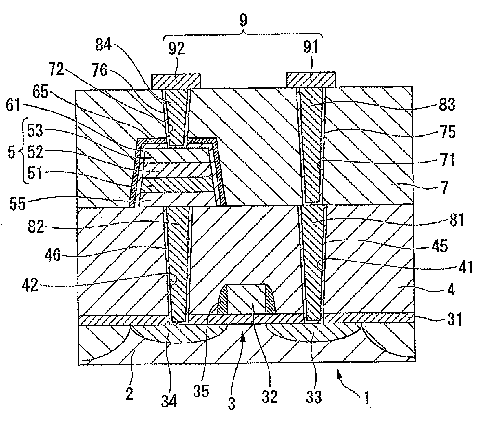
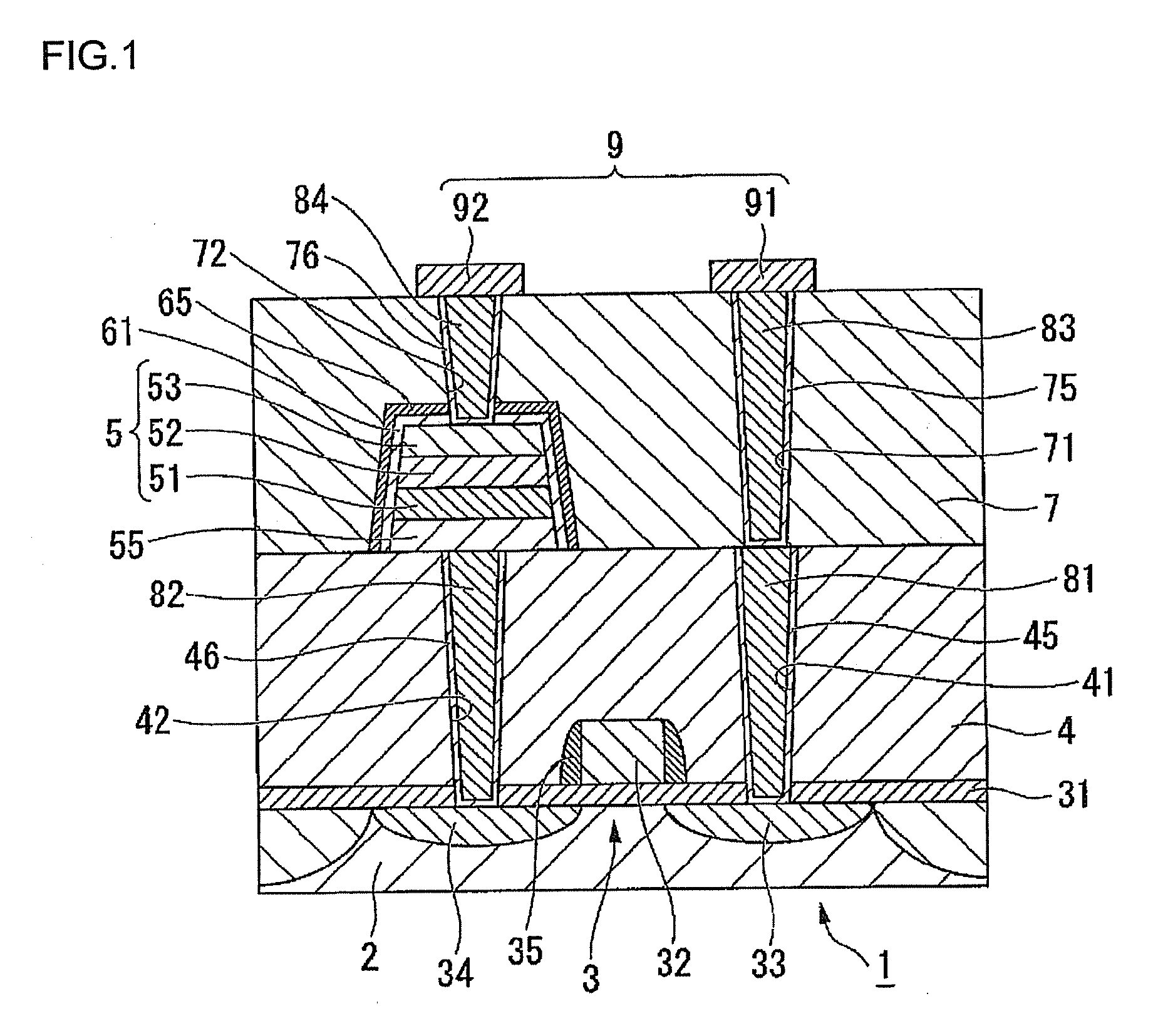
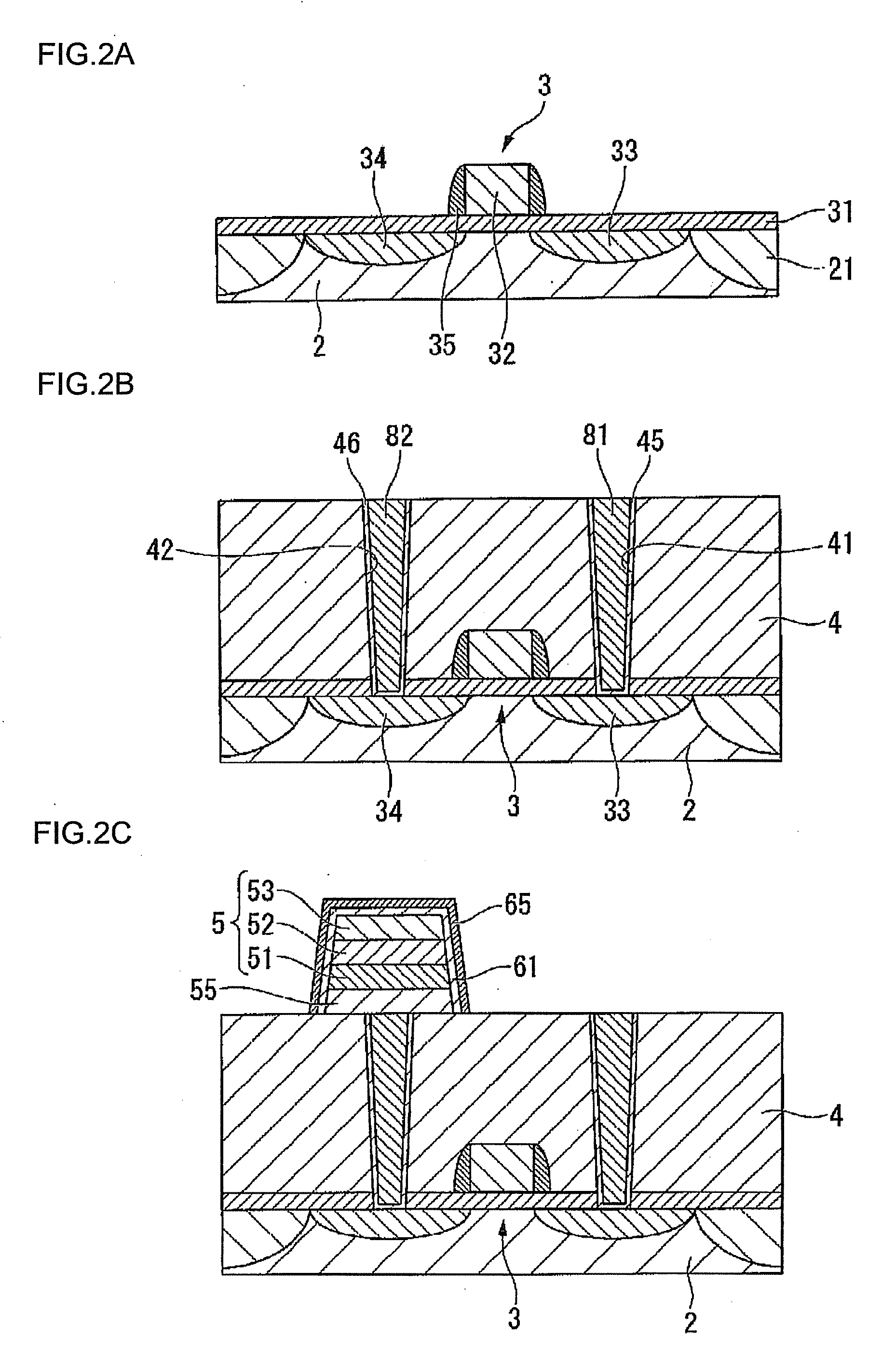
[0032]FIG. 1 is a cross-sectional structural view of a memory cell using a ferroelectric capacitor in accordance with an embodiment of the invention. As shown in FIG. 1, the memory cell 1 is equipped with a switching transistor 3 formed on a semiconductor substrate 2 that may be composed of single crystal silicon or the like, a base dielectric film 4 covering the switching transistor 3, a charg...


PUM


Abstract

A method for manufacturing a ferroelectric capacitor includes the steps of: forming a base dielectric film on a substrate, and forming a first plug conductive section in the base dielectric film at a predetermined position; forming, on the base dielectric film, a charge storage section formed from a lower electrode, a ferroelectric film and an upper electrode; forming a stopper film from an insulation material that covers the charge storage section; forming a hydrogen barrier film that covers the stopper film; forming an interlayer dielectric film on the base dielectric film including the hydrogen barrier film; forming, in the interlayer dielectric film, a first contact hole that exposes the first plug conductive section; forming a second contact hole that exposes the upper electrode of the charge storage section by successively etching the interlayer dielectric film, the hydrogen barrier film and the stopper film by using a resist pattern as a mask, and then removing the resist pattern by a wet cleaning treatment; forming an adhesion layer from a conductive material having hydrogen barrier property inside the second contact hole in a manner to cover an upper surface of the upper electrode; forming a second plug conductive section inside the first contact hole; and forming a third plug conductive section inside the second contact hole, wherein the stopper film is formed from a material having a lower etching rate for a cleaning liquid used for the wet cleaning treatment to remove the resist pattern than an etching rate of the hydrogen barrier film for the cleaning liquid.

Description

[0001]The entire disclosure of Japanese Patent Application No. 2007-137685, filed May 24, 2007 is expressly incorporated by reference herein.BACKGROUND[0002]1. Technical Field[0003]The present invention relates to methods for manufacturing ferroelectric capacitors, and also relates to ferroelectric capacitors.[0004]2. Related Art[0005]Ferroelectric memory devices (FeRAM) are nonvolatile memory devices that use spontaneous polarization of ferroelectric material and are capable of low voltage and high speed operations, and their memory cells can be each formed from one transistor and one capacitor (1T / 1C). Accordingly, ferroelectric memory devices can achieve integration at the same level of that of DRAM, and are therefore expected as large-capacity nonvolatile memories.[0006]Each memory cell of a ferroelectric memory device generally has a stacked structure in which a transistor, a base dielectric film, a charge storage section, an interlayer dielectric film and a wiring layer are su...

Claims


Application Information

Patent Timeline
IPC IPC(8): H01L27/108H01L21/02
CPCH01L27/11502H01L27/11507H01L28/55H01L28/57H10B53/30H10B53/00
Inventor URUSHIDO, TATSUHIRO
Owner SEIKO EPSON CORP
Why Eureka
Try Eureka