Method of manufacturing semiconductor device

a manufacturing method and technology of semiconductor devices, applied in the direction of cleaning processes and apparatus, chemistry apparatus and processes, transistors, etc., can solve the problems of inability to avoid variations in the resistance of the silicide layer, the electrical properties of the nickel silicide layer are reduced, and the resistance of the nickel silicide layer is not easy to achieve. , the effect of improving reliability

Active Publication Date: 2007-10-11
RENESAS ELECTRONICS CORP
View PDF5 Cites 243 Cited by
  • Summary
  • Abstract
  • Description
  • Claims
  • Application Information

AI Technical Summary

Benefits of technology

[0010]An object of one invention according to the present application is to provide a technology capable of manufacturing a semiconductor device having improved reliability and production yield by reducing variations in the electrical properties of a nickel silicide layer.
[0020]The heat treatment at the first temperature is advantageous because it needs a relatively low temperature so that an apparatus having a relatively simple structure can be employed and an adequate through-put can be ensured. It is also advantageous because the residue can be relatively completely (to an extent sufficient to avoid spread of contamination which will otherwise occur by handling) removed from the back surface and side surface by this treatment and does not interfere with the handling of the wafer. The heat treatment at the second temperature is necessary when the product containing a non-stoichiometric composition, if any, sometimes increases the evaporation temperature and in addition, it sometimes increases the effective evaporation temperature on the practical upper surface of the wafer having a complex structure, depending on the geomorphologic feature.
[0029]This method is advantageous because the cleaning residues can be removed by the single heat treatment in one chamber and therefore the treatment chamber of the apparatus can be used effectively.
[0034]The above-described method is advantageous because the cleaning residues can be removed by single heat treatment so that a sufficient through-put can be ensured.
[0045]Since variations in the electrical properties of a nickel silicide layer can be reduced, a semiconductor element having improved reliability and production yield can be obtained.

Problems solved by technology

The nickel silicide layer formed by the salicide technology however has various technical problems which will be described below.
As a result of studying the removal of the above-described product by warming the dry-cleaned surface of the semiconductor substrate at about 100° C. which is a sublimation temperature of the product, it has however been elucidated that even warming of the semiconductor substrate at about 100° C. cannot sublimate the product completely and therefore variations in the resistance of the silicide layer cannot be avoided.

Method used


Image

  • Method of manufacturing semiconductor device
  • Method of manufacturing semiconductor device
  • Method of manufacturing semiconductor device

Examples


embodiment 2

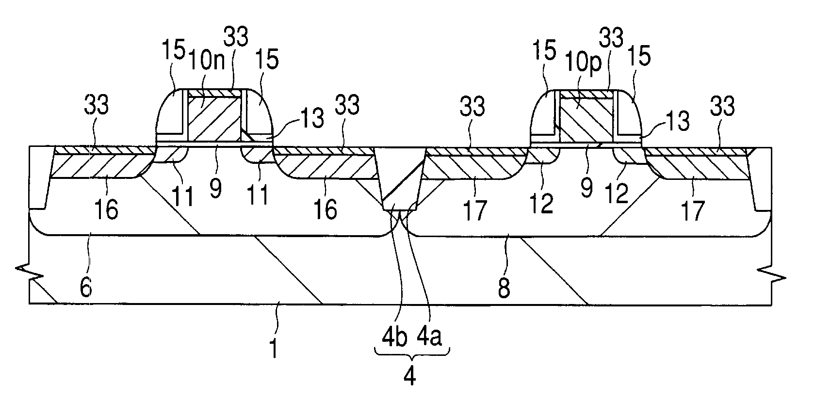
[0121]As described above in Embodiment 1, the dry cleaning treatment performed in the step of forming the nickel silicide layer 33 leaves a product over the main surface of the semiconductor wafer SW, and portions of the side surface and back surface thereof. A product having a composition of (NH4)2SiF6 is removed by heating the semiconductor wafer SW at a temperature of from 100 to 150° C. by the shower head 27c, with which the dry cleaning treatment chamber 27 is equipped, set at 180° C., followed by the removal of a product having a composition slightly different from (NH4)2SiF6 by heating in the heat treatment chamber 25 or 26 at a temperature greater than 150° C.

[0122]In Embodiment 2 according to the present invention, the product having a composition (NH4)2SiF6 and the product having a composition slightly different from (NH4)2SiF6 are removed by setting the temperature of a shower head 27CH, with which the dry cleaning treatment chamber 27 is equipped with, to greater than 18...


PUM

PropertyMeasurementUnit
temperatureaaaaaaaaaa

Abstract

Provided is a method of manufacturing a semiconductor device. After a semiconductor wafer is placed over a wafer stage with which a dry cleaning chamber of a film forming apparatus is equipped, dry cleaning treatment is given over the surface of the semiconductor wafer with a reducing gas. Then, the semiconductor wafer is heat treated at a first temperature of from 100 to 150° C. by using a shower head kept at 180° C. The semiconductor wafer is then vacuum-transferred to a heat treatment chamber, wherein the semiconductor wafer is heat treated at a second temperature of from 150 to 400° C. A product remaining over the main surface of the semiconductor wafer is thus removed. The present invention makes it possible to manufacture a semiconductor device having improved reliability and production yield by reducing variations in the electrical properties of a nickel silicide layer.

Description

CROSS-REFERENCE TO RELATED APPLICATIONS[0001]The disclosure of Japanese Patent Application No. 2006-107780 filed on Apr. 10, 2006 including the specification, drawings and abstract is incorporated herein by reference in its entirety.BACKGROUND OF THE INVENTION[0002]The present invention relates to a manufacturing technology of a semiconductor device, in particular, to a technique effective when applied to the manufacture of a semiconductor element having a nickel silicide layer.[0003]With increasing integration density of semiconductor devices, field effect transistors (Metal Insulator Semiconductor Field Effect Transistors) are miniaturized according to the scaling rule. The miniaturization of field effect transistors however does not lead to a high-speed operation because of an increase in the resistance of a gate or source and drain. For example, in field effect transistors having a gate length of 0.2 μm or less, a salicide technology of forming a low-resistance silicide layer, f...

Claims


Application Information

Patent Timeline
Patent Type & Authority Applications(United States)
IPC IPC(8): B08B6/00
CPCH01L21/02057H01L21/02068H01L21/67167H01L21/67184H01L21/67207Y10S438/906H01L21/823842H01L29/665H01L29/6659H01L29/7833H01L21/823835H01L29/772
Inventor FUTASE, TAKUYATSUGANE, HIDEAKIKIMOTO, MITSUOSUZUKI, HIDENORI
Owner RENESAS ELECTRONICS CORP
Why Eureka
Try Eureka