Method for computing the sensitivity of a VLSI design to both random and systematic defects using a critical area analysis tool

Inactive Publication Date: 2007-10-11
GLOBALFOUNDRIES INC
View PDF5 Cites 15 Cited by
  • Summary
  • Abstract
  • Description
  • Claims
  • Application Information

AI Technical Summary

Benefits of technology

[0017] Accordingly, embodiments herein use the basic framework of critical area analysis to measure sensitivity to random defects. To account for systematic defects, the analysis is modified by giving higher weight to th

Problems solved by technology

In the design and manufacture of very large scale integration (VLSI) semiconductor chips, two types of yield detractors in the manufacturing process are random defects and systematic defects.
Systematic defects—also known as process-sensitive sites—constitute electrical faults that arise because of the inherent difficulty of repeatedly building certain structures in a given manufacturing technology.
By contrast, systematic defects result because some structures are more difficult to manufacture than others.
In a given process, certain geometrical configurations can be particularly susceptible to yield problems.
For example: certain combinations of wide metal lines and narrow metal lines might interact in a certain way because of the polish stage and lead to electrical shorts and thus non-functional parts.
In general, there is no simple way to measure the sensitivity of a design to

Method used


Image

  • Method for computing the sensitivity of a VLSI design to both random and systematic defects using a critical area analysis tool
  • Method for computing the sensitivity of a VLSI design to both random and systematic defects using a critical area analysis tool
  • Method for computing the sensitivity of a VLSI design to both random and systematic defects using a critical area analysis tool

Examples


Example

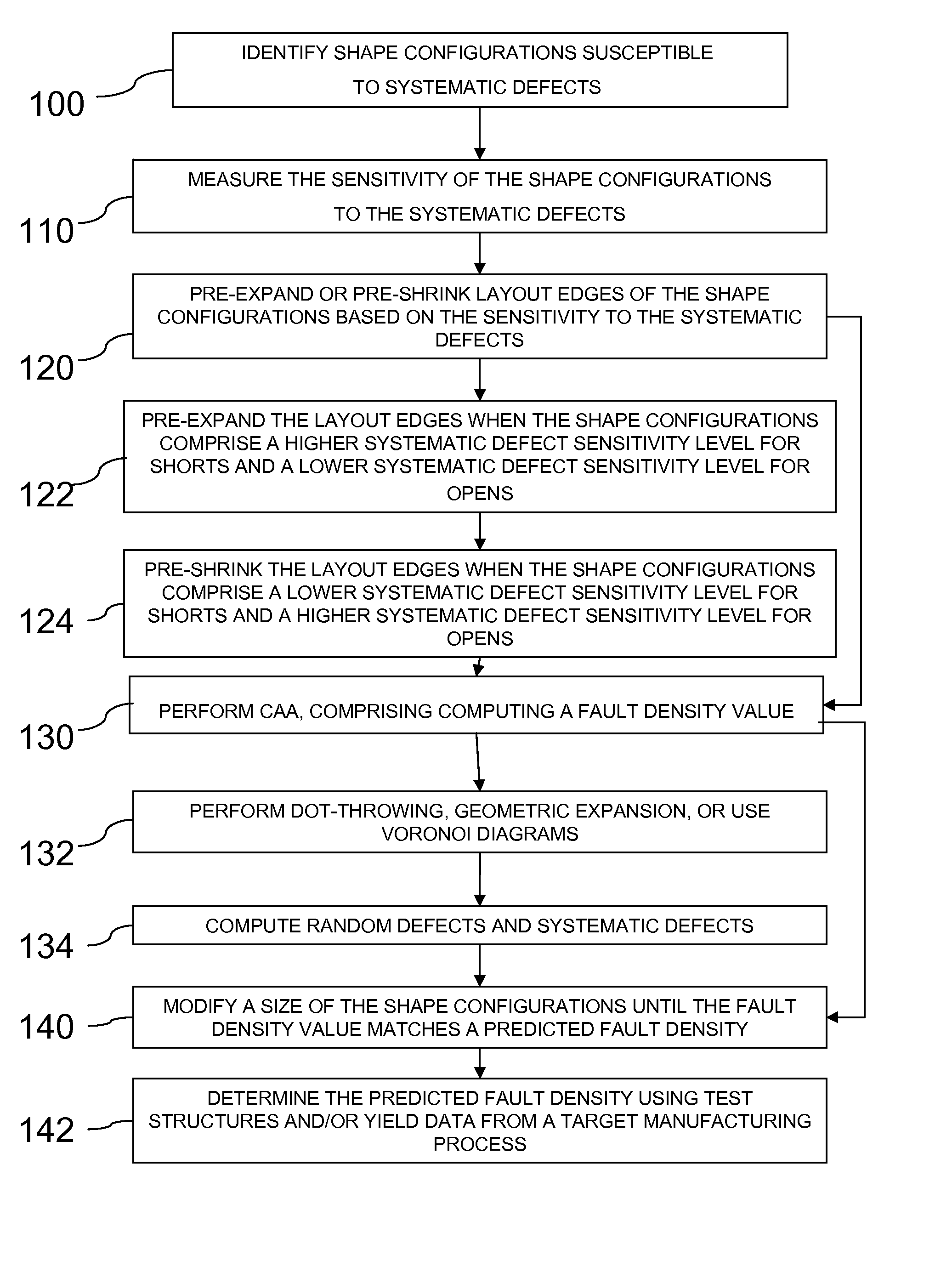
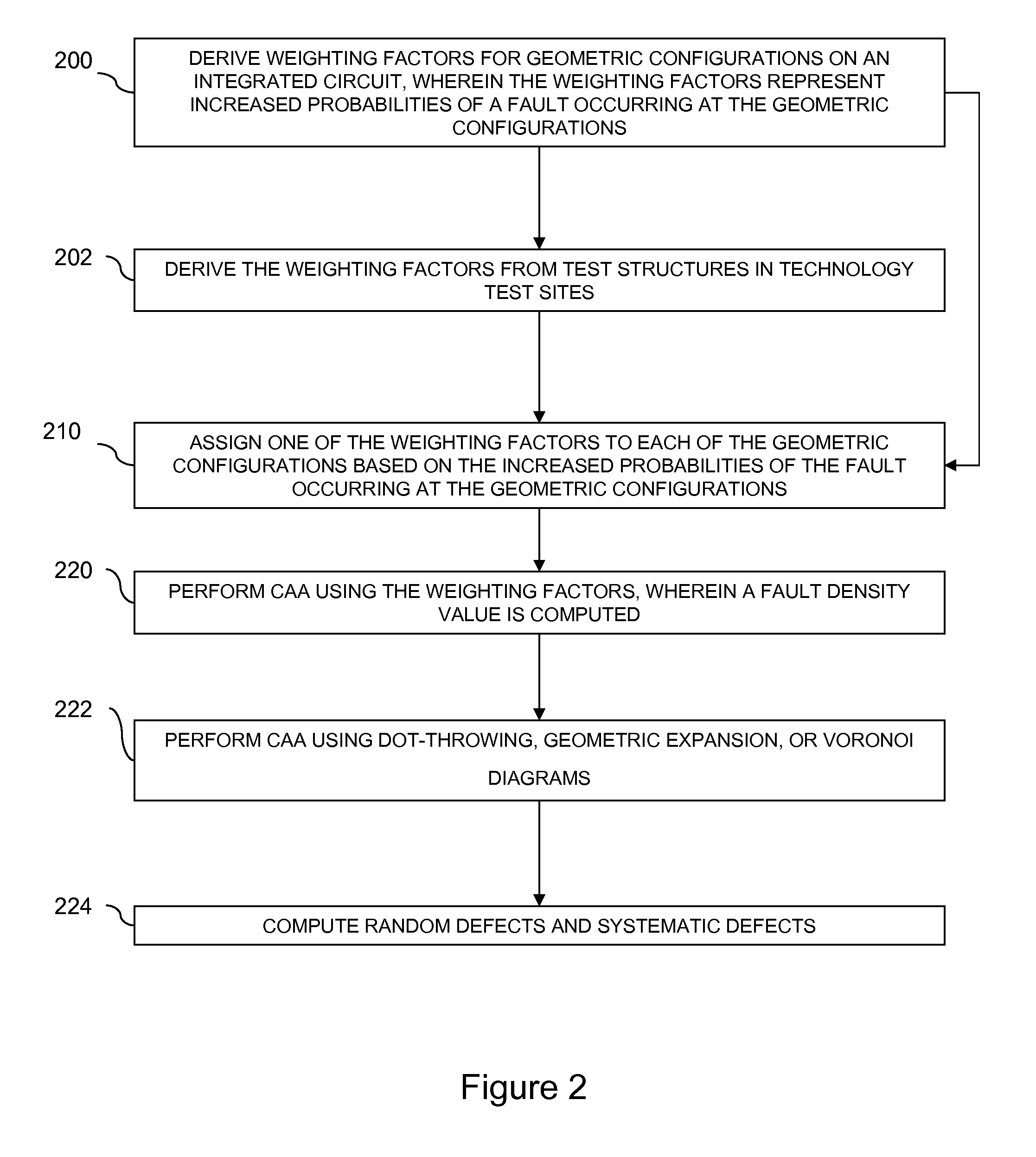
[0022] The embodiments of the invention and the various features and advantageous details thereof are explained more fully with reference to the non-limiting embodiments that are illustrated in the accompanying drawings and detailed in the following description. It should be noted that the features illustrated in the drawings are not necessarily drawn to scale. Descriptions of well-known components and processing techniques are omitted so as to not unnecessarily obscure the embodiments of the invention. The examples used herein are intended merely to facilitate an understanding of ways in which the embodiments of the invention may be practiced and to further enable those of skill in the art to practice the embodiments of the invention. Accordingly, the examples should not be construed as limiting the scope of the embodiments of the invention.

[0023] Accordingly, embodiments herein use the basic framework of critical area analysis to measure sensitivity to random defects. To account ...


PUM


Abstract

A method of estimating integrated circuit yield comprises providing an integrated circuit layout and a set of systematic defects based on a manufacturing process. Next, the method represents a systematic defect by modifying structures in the integrated circuit layout to create modified structures. More specifically, for short-circuit-causing defects, the method pre-expands the structures when the structures comprise a higher systematic defect sensitivity level, and pre-shrinks the structures when the structures comprise a lower systematic defect sensitivity level. Following this, a critical area analysis is performed on the integrated circuit layout using the modified structures, wherein dot-throwing, geometric expansion, or Voronoi diagrams are used. The method then computes a fault density value, random defects and systematic defects are computed. The fault density value is subsequently compared to a predetermined value, wherein the predetermined value is determined using test structures and/or yield data from a target manufacturing process.

Description

BACKGROUND [0001] 1. Field of the Invention [0002] Embodiments of the invention provide a method for computing the sensitivity of a VLSI design to both random and systematic defects using a critical area analysis tool. [0003] 2. Description of the Related Art [0004] In the design and manufacture of very large scale integration (VLSI) semiconductor chips, two types of yield detractors in the manufacturing process are random defects and systematic defects. Random defects refer to electrical faults (e.g., opens and shorts) caused by foreign material or impurities. Systematic defects—also known as process-sensitive sites—constitute electrical faults that arise because of the inherent difficulty of repeatedly building certain structures in a given manufacturing technology. [0005] Random defects are predicted using critical area. Critical area is a mathematical measure of the sensitivity of a VLSI layout to random defects. It is a function of the sizes of features and the spaces between f...

Claims


Application Information

Patent Timeline
IPC IPC(8): G06F17/50G06F19/00
CPCG06F17/5081G06F30/398
Inventor BICKFORD, JEANNE P.HIBBELER, JASON D.KOEHL, JUERGEN
Owner GLOBALFOUNDRIES INC
Why Eureka
Try Eureka