

Method for manufacturing solid-state image pickup element and solid-state image pickup element
a pickup element and solid-state technology, applied in the direction of basic electric elements, electrical equipment, semiconductor devices, etc., can solve the problems of reducing sensitivity, poor coverage of the resulting film, and affecting the efficiency of focusing light on the light-receiving portion, so as to improve light-focusing efficiency and reduce the aspect ratio , the effect of high sensitivity
- Summary
- Abstract
- Description
- Claims
- Application Information
AI Technical Summary
Benefits of technology
Problems solved by technology
Method used
Image

Examples
Embodiment Construction
[0041] Preferred embodiments of a method for manufacturing a solid-state image pickup element and a solid-state image pickup element according to the present invention will be explained in detail below with reference to the accompanying drawings.
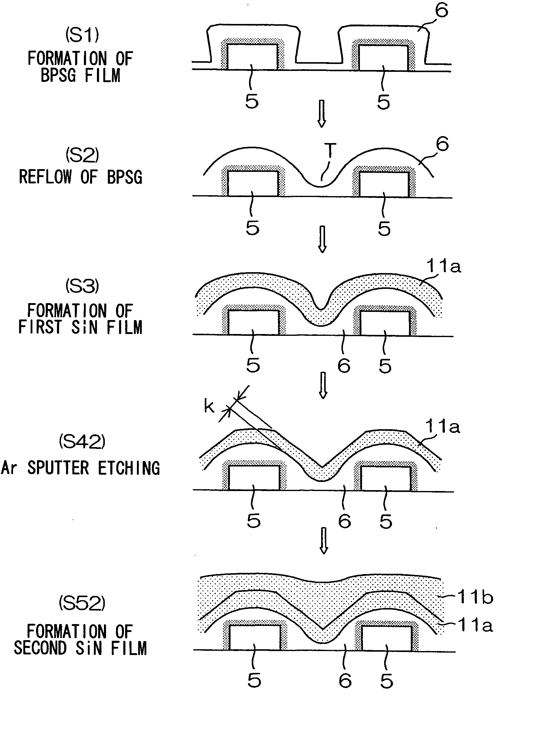
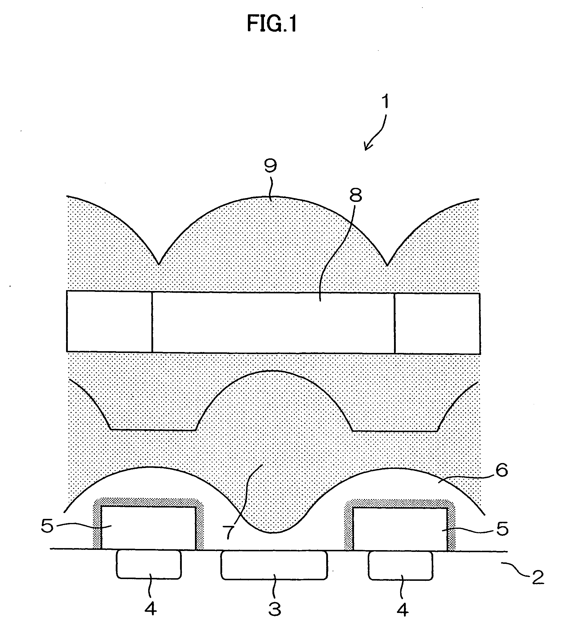
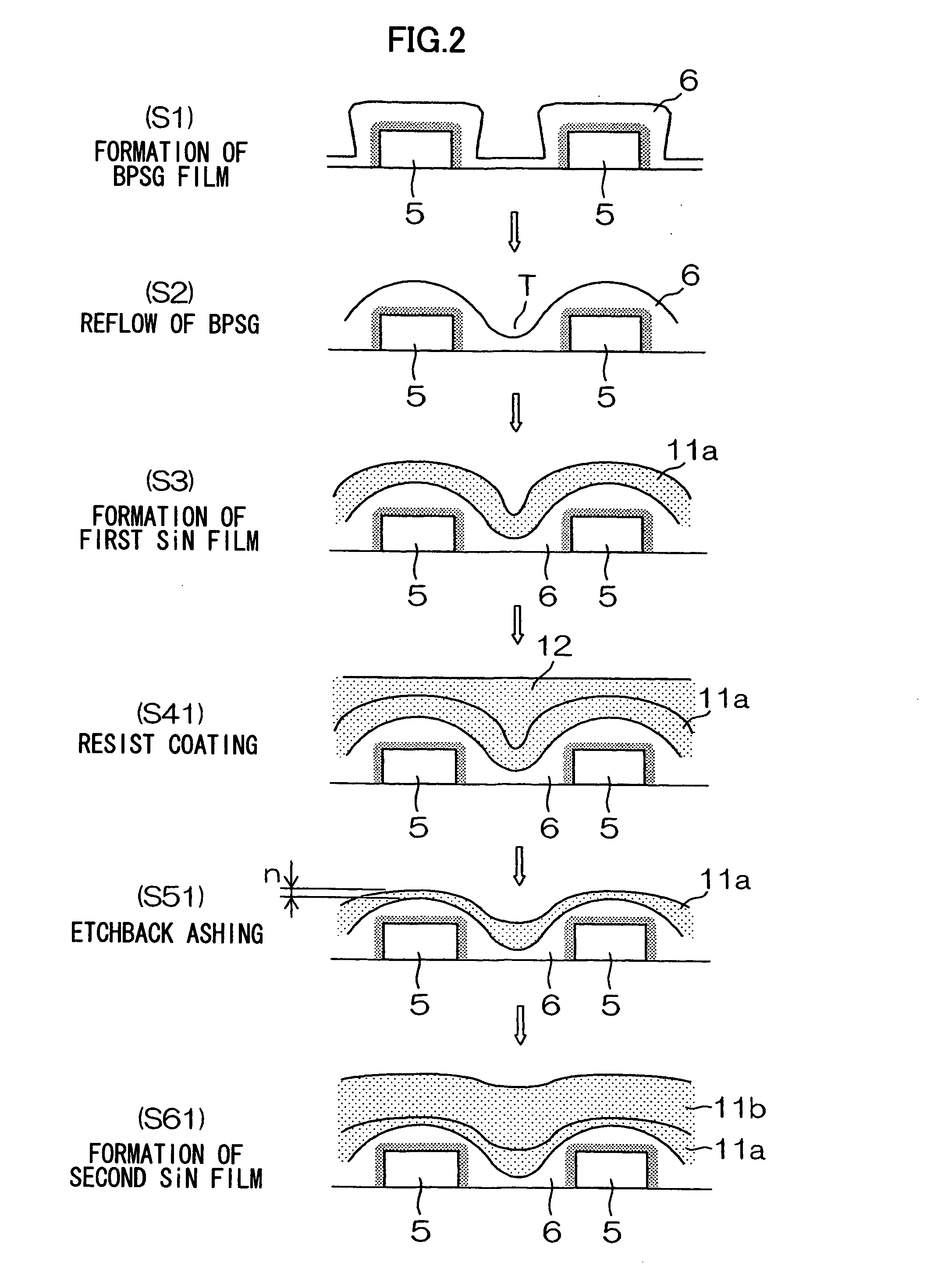
[0042] The configuration of a solid-state image pickup element according to the present invention will be explained first. In a solid-state image pickup element 1 shown in FIG. 1, an n-type photodiode 3 and an n-type transfer channel 4 serving as solid-state image pickup element components are formed in the surface of a semiconductor substrate 2 obtained by forming a p-type well layer on an n-type substrate. A transfer electrode 5 is formed above the transfer channel 4 through an insulating film made of, e.g., silicon oxide.
[0043] The transfer electrode 5 is formed of, e.g., polysilicon and covered with a light-shielding film made of W (tungsten) which has an opening portion on the photodiode 3. A BPSG film 6 which is formed by atmospheric...
PUM
 Abstract
Description
Claims
Application Information