

Method of forming compressive nitride film and method of manufacturing metal oxide semiconductor
a technology of compressive nitride and metal oxide, which is applied in the direction of semiconductor devices, basic electric elements, electrical equipment, etc., can solve the problems of obtaining a film with a higher compressive stress, and the most well-known as-deposit technology in the world can only reach 1.6 gpa, so as to improve the structural stress of both pmos and nmos, increase the current gain, and increase the drive current gain
- Summary
- Abstract
- Description
- Claims
- Application Information
AI Technical Summary
Benefits of technology
Problems solved by technology
Method used
Image

Examples
first embodiment
The First Embodiment
[0037] A method of manufacturing a compressive nitride film according to a first embodiment of the present invention includes performing a CVD process to form a nitride film on a substrate. The CVD process is, for example, PECVD. Also, it is required to add a certain gas, selected from among Ar, N2, Kr, Xe, and mixtures thereof, during the CVD process. For example, when the certain gas is a combination of Ar and N2, the flow of Ar is about 100 sccm-5000 sccm; the flow of N2 is about 1000 sccm-30000 sccm. Moreover, the low frequency (LF) Power used in the CVD process is preferably about 50 W-3000 W.
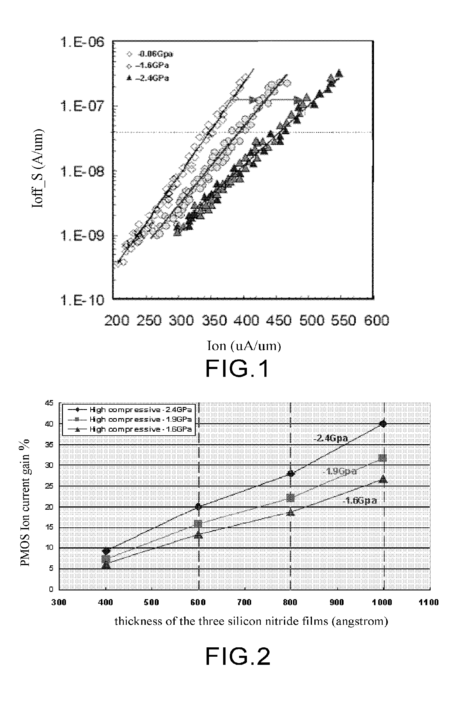
[0038] Table 1 below is a parameter table for the process of the method of the first embodiment (test example 1 and 2) compared with a conventional method (comparative example) without adding a certain gas of the present invention during the CVD process.
TABLE 1SiH4NH3ArN2HFLF (W)Stress(sccm)(sccm)(sccm)(sccm)(W)(Bias)(GPa)Compara-2403200040001000−0.07tiveexampleTest6...
second embodiment
The Second Embodiment
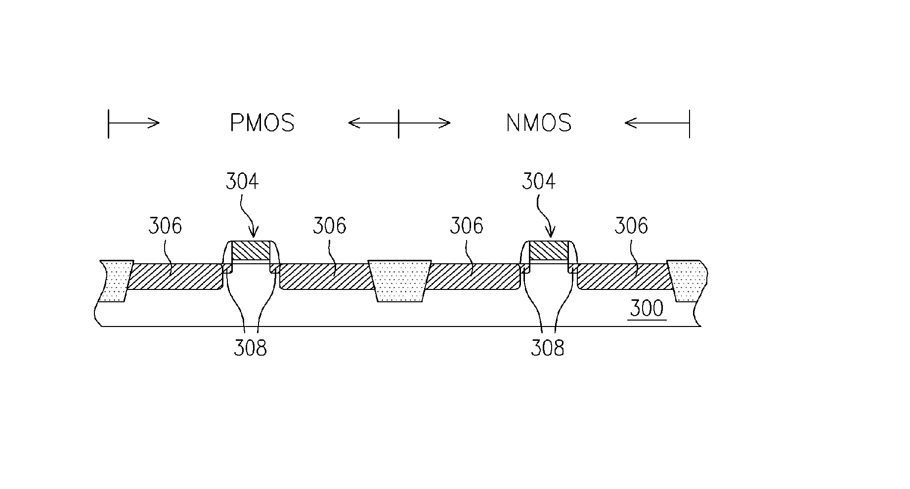
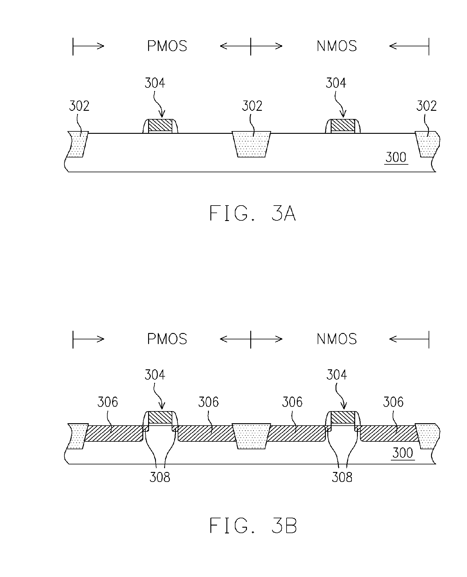
[0043]FIGS. 3A to 3D are schematic cross-sectional views of a process of manufacturing a MOS according to a second embodiment of the present invention.
[0044] Referring to FIG. 3A, a substrate 300 is first provided, which has a crystallographic direction 100> at a crystallographic plane (100). The substrate is supposed to be divided into a PMOS region and a NMOS region by a plurality of isolating structures 302. Gate structures 304 have already been formed on the substrate 300. The gate structure 304 substantially comprises a gate dielectric layer, a gate on the gate dielectric layer, and a spacer formed in the sidewall of the gate. Besides, other means are also included, which can be appreciated by those of ordinary skill in the technical field of the present invention through the current technique, and will not be repeated any more herein.
[0045] Then, referring to FIG. 3B, a source and a drain 306 are formed in the substrate 300 at both sides of gate structur...
third embodiment
The Third Embodiment
[0049]FIGS. 4A to 4D are schematic cross-sectional views of a process of manufacturing a MOS according to a third embodiment of the present invention.
[0050] Referring to FIG. 4A, a substrate 400 is first provided, which has a crystallographic direction 100> at a crystallographic plane (100). The substrate is supposed to be divided into a first region 400a and a second region 400b by a plurality of isolating structures 402. For example, if the first region 400a is the PMOS region, the second region 400b is the NMOS region. Then, a gate structure 404 is formed on the first region 400a and the second region 400b of the substrate 400 respectively. Thereafter, a source and a drain 406 are formed in the substrate 400 at both sides of each of the gate structures 404, and the way of forming the source and the drain 406 may be obtained with reference to the illustration of the second embodiment (shown in FIG. 3B). After that, it is decided to form a first buffer layer 40...
PUM
| Property | Measurement | Unit |
|---|---|---|
| size | aaaaa | aaaaa |
| temperature | aaaaa | aaaaa |
| thickness | aaaaa | aaaaa |
Abstract
Description
Claims
Application Information