Substrate holding system and exposure apparatus using the same

a technology of substrate and holding system, applied in the field of substrate holding system and exposure apparatus, can solve the problems of method cannot be used in vacuum ambience, deformation of wafer or damage of wafer, etc., and achieve the effect of stabilizing the flatness of the substra

Inactive Publication Date: 2007-10-25
CANON KK
View PDF4 Cites 6 Cited by
  • Summary
  • Abstract
  • Description
  • Claims
  • Application Information

AI Technical Summary

Benefits of technology

[0019] In accordance with the present invention, flatness correction of a substrate can be stabilized.

Problems solved by technology

If the substrate holding precision is insufficient, a printed pattern or an overlay precision is degraded.
Although it has a feature of being less susceptible to the influence of the environment, since only the outer periphery of the wafer is held, there is a problem of deformation of the wafer or damaging the wafer.
However, this method cannot be used in a vacuum ambience, and it cannot be applied to apparatuses using a vacuum.
Substrates such as wafers to be processed in semiconductor manufacturing steps are not always uniform in a plane, and, in some cases, they may have a large warp as a result of a film forming process, for example.
However, as described, this technique cannot be used in a system operated in a vacuum ambience.
On the other hand, electrostatic attraction cannot easily meet such warping of a wafer, as compared with the vacuum attraction.
However, if a wafer is warped irregularly, correction is difficult to achieve.
If an electrical discharge occurs between the substrate and the substrate attracting device, it may cause damage to the substrate or breakage of devices on the substrate.
Furthermore, the discharge may create dust particles, which contaminate the substrate and the substrate attracting device.
However, if the voltage for electrostatic attraction is made low (not greater than 300 V), a sufficient attraction force is not produced and, therefore, it is unable to achieve secure flatness correction of a warped substrate.

Method used


Image

  • Substrate holding system and exposure apparatus using the same
  • Substrate holding system and exposure apparatus using the same
  • Substrate holding system and exposure apparatus using the same

Examples


embodiment 1

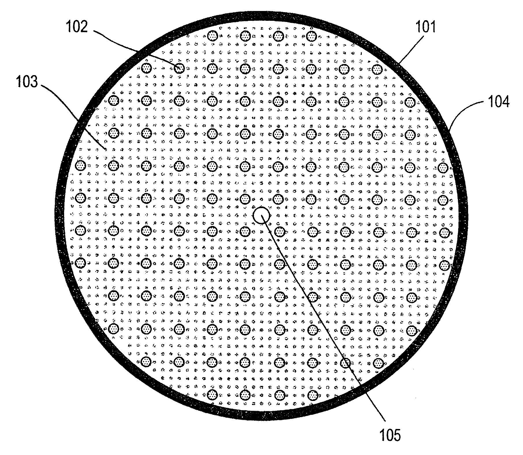
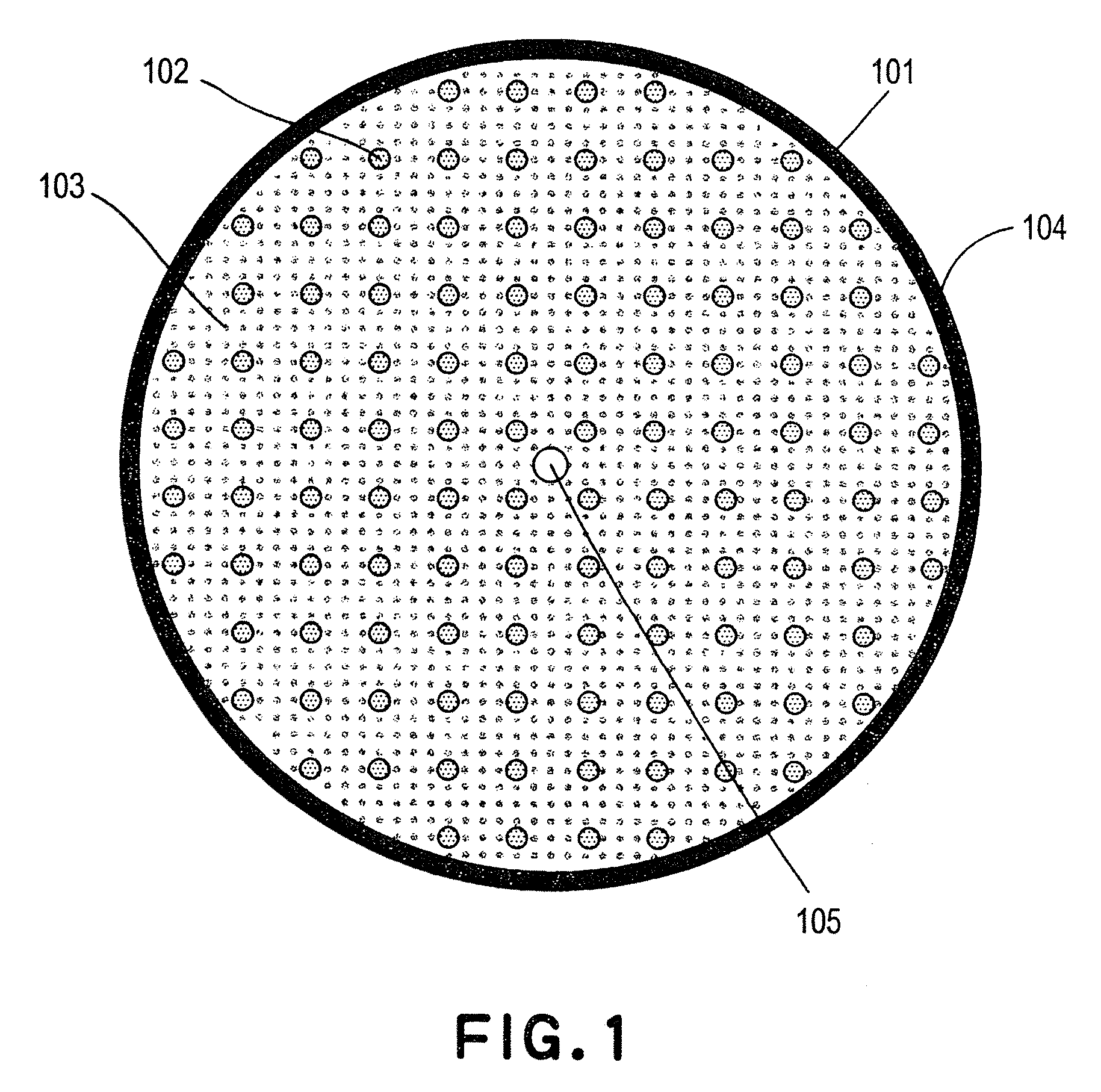
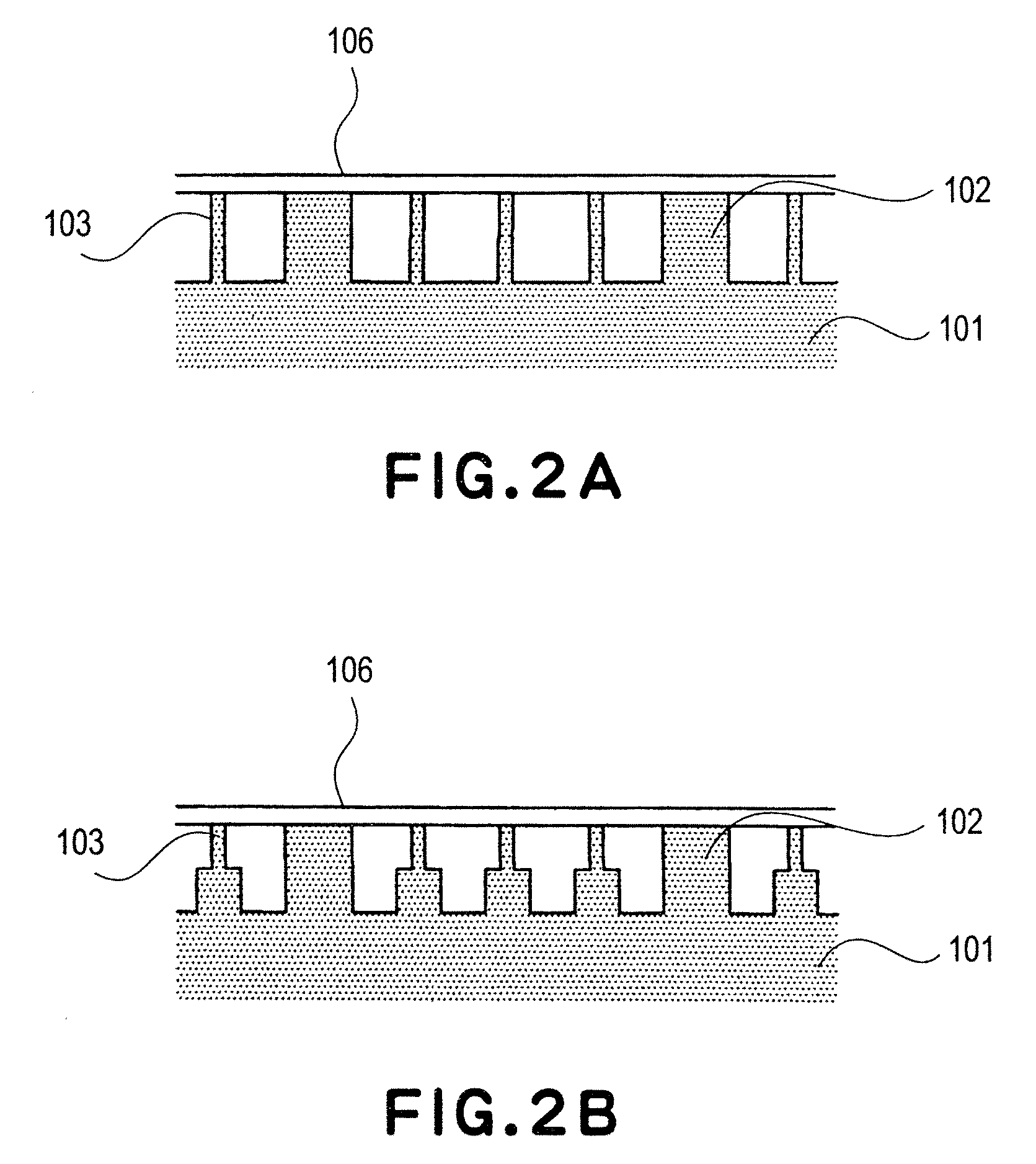
[0036]FIGS. 1, 2A and 2B illustrate the structure of a substrate attracting device according to a first embodiment of the present invention. In FIG. 1, a substrate attracting portion (chuck) 101 includes protrusions (first protrusions) 102 mainly for electrostatic attraction, protrusions (second protrusions) 103 mainly for vacuum attraction, a ring-like rim 104 adapted to apply a vacuum between the substrate and the substrate attracting portion, and an exhaust port 105. The total area of the substrate carrying surface as defined by the group of protrusions 103 for the vacuum attraction is made larger than the total area of the substrate carrying surface as defined by the group of protrusions 102 for electrostatic attraction. Furthermore, each protrusion 103 for vacuum attraction has a smaller carrying surface area than the protrusion 102 for electrostatic attraction, and also the interval of the protrusions 103 is smaller than that of the protrusions 102. Each of the protrusions 102...

embodiment 2

[0043]FIGS. 3A, 3B, 4A and 4B illustrate the structure of a substrate attracting device according to a second embodiment of the present invention. In the second embodiment, a substrate attracting portion (chuck) 201 having at least an electrostatic attracting mechanism is provided with a power supply terminal 202 for during conveyance of the substrate attracting portion, and a power supply terminal 203 for during fixation (stationary) of the substrate attracting portion.

[0044]FIGS. 3A and 3B show a power supplying line 206 for the substrate attracting portion 201 when the same is being conveyed by a conveying hand 205. The power supply terminal 202 for during conveyance is provided at a location separate from the power supply terminal 203 for during fixation of the substrate attracting portion, and electrical power is supplied from the power supplying line 206 of the conveying hand 205. The conveying hand 205 may have any arbitrary shape, and also the power supply terminal 202 may ...

embodiment 3

[0050]FIGS. 5 and 6 illustrate the structure of a substrate correcting device according to a third embodiment of the present invention. In the third embodiment, a substrate attracting portion (chuck) 301, having at least an electrostatic attracting mechanism, is provided with electrodes 302, which are arrayed in a stripe-like fashion, as shown inFIG. 5, and also, means for applying a voltage to each electrode is provided. Although, in FIG. 5, the shape of other substrate carrying surfaces is defined by protrusions 303 and a ring-like rim 304, any other structure may be used. However, for a secured attraction force, it is preferable to provide electrodes throughout the whole carrying surface as much as possible.

[0051] In this embodiment, as shown in FIG. 6, there is a chuck rotating mechanism 36 for rotationally moving the chuck 301 to thereby change the orientation of the stripe-like electrodes 302 as desired. In FIG. 6, the rotating mechanism 316 is connected to the chuck supporti...


PUM

PropertyMeasurementUnit
pressureaaaaaaaaaa
discharge voltageaaaaaaaaaa
pressureaaaaaaaaaa

Abstract

A substrate holding system for holding a substrate based on vacuum attraction and electrostatic attraction including a rim configured to support the substrate, a protrusion for the electrostatic attraction, configured to support the substrate inside the rim, and a protrusion for the vacuum attraction, configured to support the substrate inside the rim. A substrate supporting surface area of the protrusion of the electrostatic attraction is larger than a substrate supporting surface area of the protrusion for the vacuum attraction.

Description

[0001] This application is a divisional application of copending U.S. patent application Ser. No. 10 / 952,732, filed Sep. 30, 2004.FIELD OF THE INVENTION AND RELATED ART [0002] This invention relates to a substrate holding technique suitable for safely and securely holding even a warped substrate. More particularly, the invention concerns a substrate holding technique suitably usable in an apparatus, such as a semiconductor exposure apparatus using extreme ultraviolet (EUV) light or a charged-particle beam, wherein a substrate is processed in a vacuum or a reduced pressure ambience. [0003] The density and fineness of semiconductor devices are advancing much more, and a substrate holding system is required to have a capability of holding a substrate at a higher precision. If the substrate holding precision is insufficient, a printed pattern or an overlay precision is degraded. [0004] Conventionally, a substrate such as a wafer is held in accordance with a mechanical holding method or ...

Claims


Application Information

Patent Timeline
Patent Type & Authority Applications(United States)
IPC IPC(8): H01L21/683B23Q3/08G03F7/20H01L21/027H02N13/00
CPCG03F7/70708G03F7/70783G03F7/707H01L21/6831H01L21/6838H01L21/683
Inventor ITO, ATSUSHIEMOTO, KEIJI
Owner CANON KK
Why Eureka
Try Eureka