Universal CMOS device leakage characterization system

Active Publication Date: 2007-11-01
MARVELL ASIA PTE LTD
View PDF3 Cites 10 Cited by
  • Summary
  • Abstract
  • Description
  • Claims
  • Application Information

AI Technical Summary

Benefits of technology

[0025] It is still another object to provide a simple and small monitoring system that

Problems solved by technology

As the scaling of integrated circuit continues to progress, CMOS devices become prone to many different types of leakage problems.
Current technology having a gate dielectric thinner than 10 nm, a channel length shorter than 50 nm, a junction depth thinner than 20 nm, the threshold voltage of fast devices below 200 mV are typically subject to serious leakage related problems.
However, the apparatus described does not characterize other types of leakages, such as junction leakage, gate dielectric leakage.
It neither addresses the problem of monitoring and quantifying the sub-threshold leakage of PMOS devices.
The proposed approach suffers from a serious problem, in that when the gate shows either a catastrophic failure or a broken gate oxide caused by pin-holes or other defects, the voltage drop exceeds a preset threshold level (e.g., ½ Vdd).
As a result, the circuit fails to shut the decoupling capacitor off.
Again, the cited patent is not suited for universal leakage characterization, since it makes no mention of

Method used


Image

  • Universal CMOS device leakage characterization system
  • Universal CMOS device leakage characterization system
  • Universal CMOS device leakage characterization system

Examples


Example

[0043] Hereinafter will be described the n-MOS and p-MOS leakage monitoring apparatus of the present invention. Since the circuit conFIGurations for testing n-MOS and p-MOS differ significantly from each other, they will be described independently.

[0044] N-MOS Leakage Measuring Apparatus

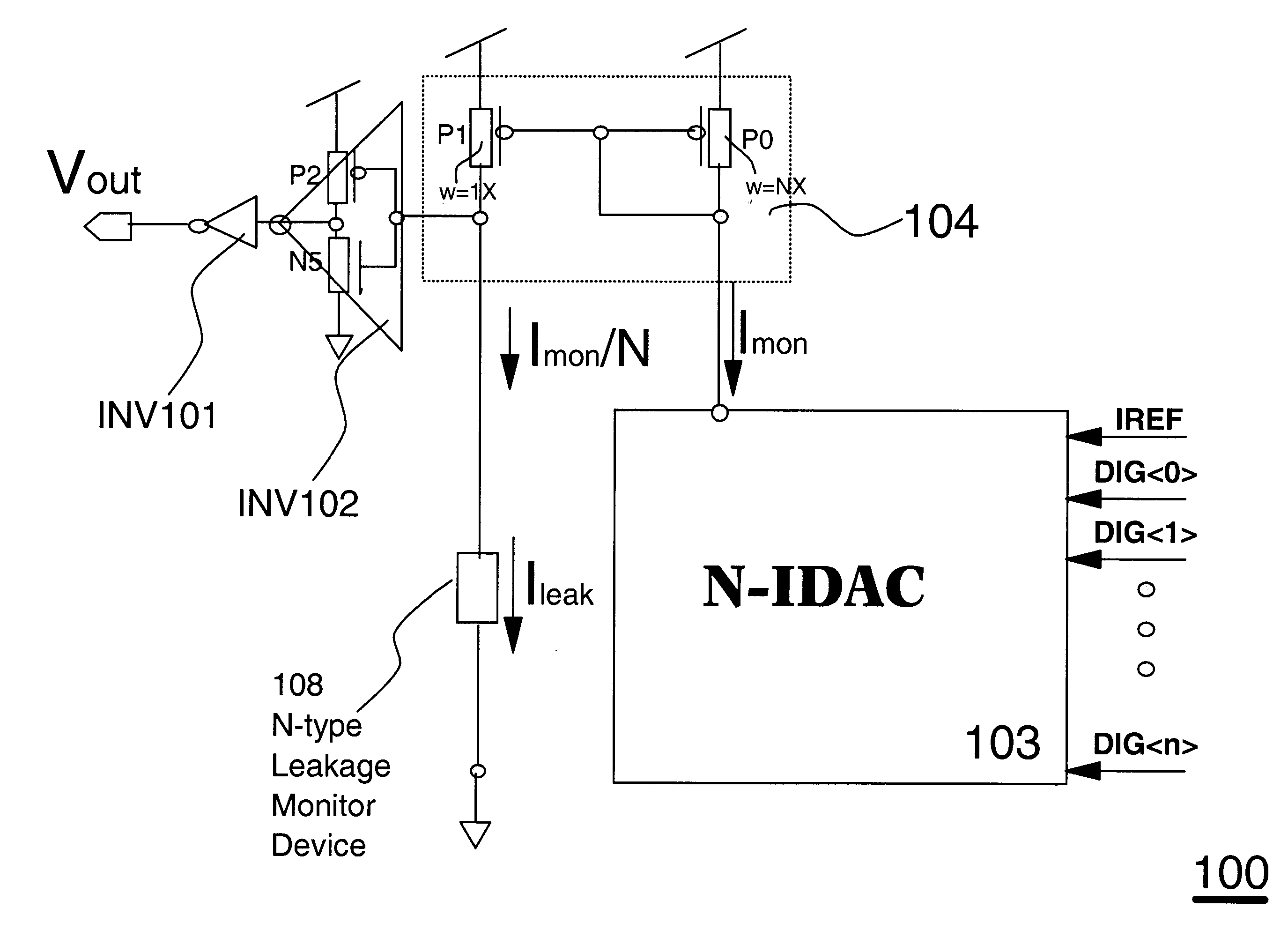
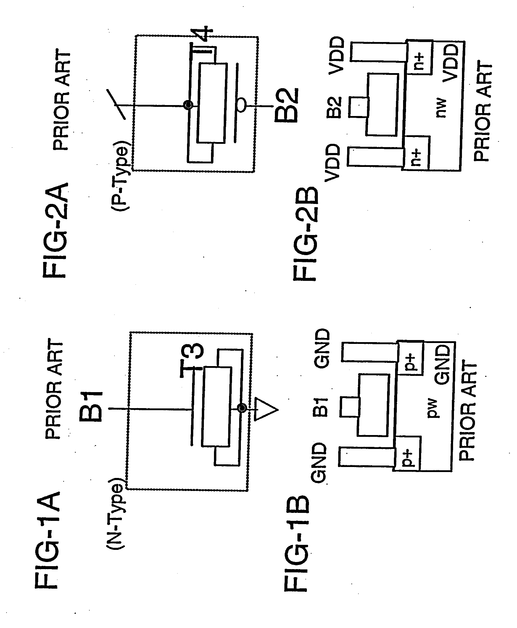
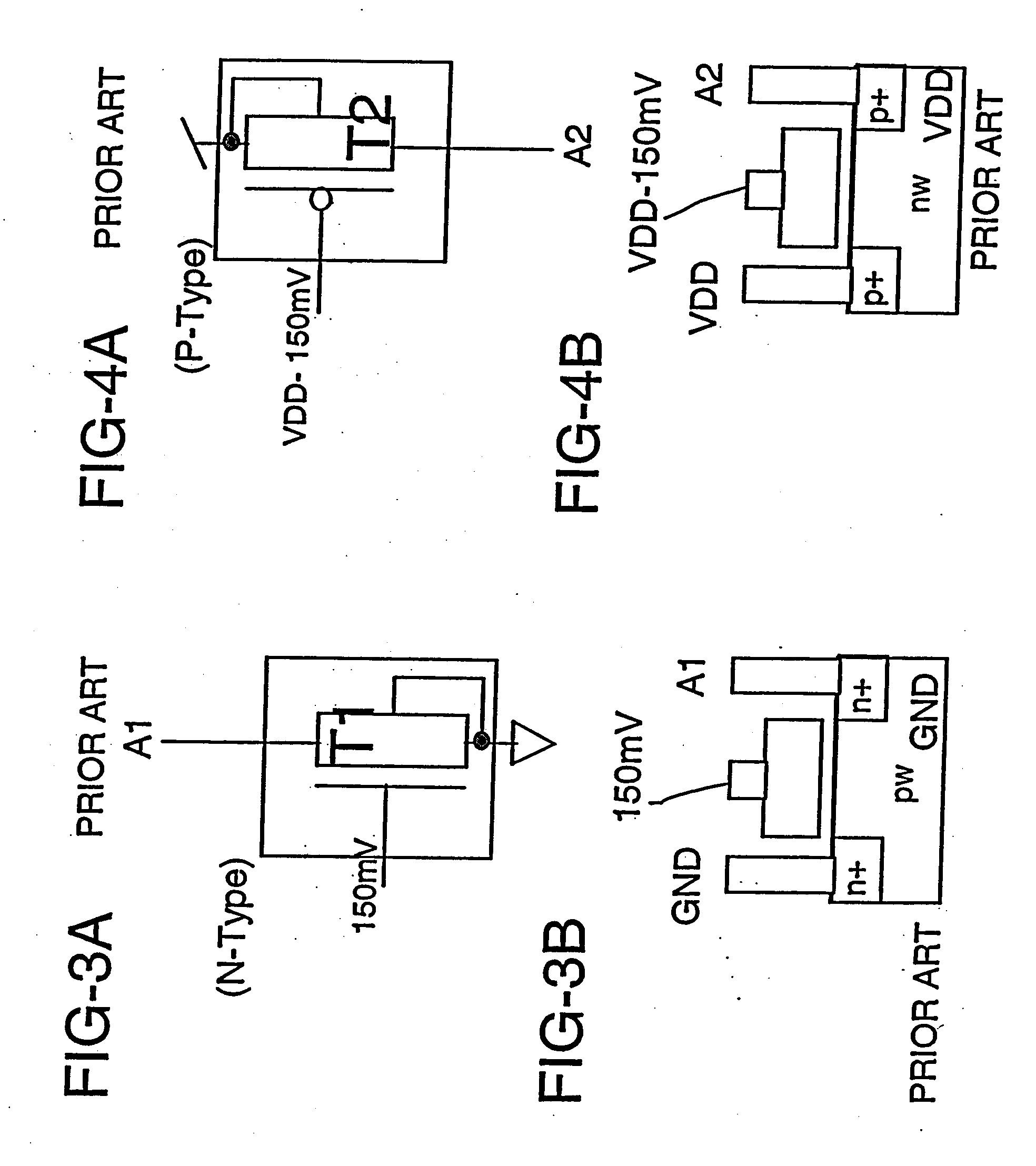
[0045] As previously stated, leakage monitoring devices of the class shown with reference to the circuits illustrated in FIGS. 1, 3 and 5, only one class of leakage, whether testing the gate, sub-threshold and junction leakage, respectively, can be tested at one time. The circuit is designed to test both normal and abnormal types of leakage for any classes of CMOS devices, which differ from each other by several orders of magnitude.

[0046] Regarding the present invention, and with reference to FIG. 7A, the digital bits DIG0>, DIG1> . . . DIG are used to size the reference current for sensing the leakage current. A binary decoding technique is, preferably, used to achieve high resolution when taking...


PUM


Abstract

The invention provides a universal leakage monitoring system (ULMS) to measure a plurality of leakage macros during the development of a manufacturing process or a normal operation period. The ULMS characterizes the leakage of both n-type and p-type CMOS devices on the gate dielectric leakage, the sub-threshold leakage, and the reverse biased junction leakage, and the like. Testing is performed sequentially from the first test macro up to the last test macro using an on-chip algorithm. When the last test macro is tested, it scans the leakage data out.

Description

BACKGROUND OF THE INVENTION [0001] This invention generally relates to the manufacture of semiconductor devices, and more particularly, to a monitoring system for detecting and characterizing various classes of leakage in CMOS devices. [0002] As the scaling of integrated circuit continues to progress, CMOS devices become prone to many different types of leakage problems. Current technology having a gate dielectric thinner than 10 nm, a channel length shorter than 50 nm, a junction depth thinner than 20 nm, the threshold voltage of fast devices below 200 mV are typically subject to serious leakage related problems. [0003] Handling leakage problems has been profusely described in the art, as for instance, in U.S. Pat. No. 6,844,750 to Hsu et al. Therein is described a leakage monitoring apparatus that first measures die leakage and then generates digital keeper control bits to improve the performance of the dynamic circuits. More specifically, the sub-threshold leakage of CMOS devices...

Claims


Application Information

Patent Timeline
IPC IPC(8): G01R31/26
CPCG01R31/2884G01R31/318577G01R31/3008
Inventor HSU, LOUIS LU-CHENPILLAI, EDWARD R.NATONIO, JOSEPHROCKROHR, JAMES D.HANSON, DAVID R.
Owner MARVELL ASIA PTE LTD
Why Eureka
Try Eureka