Touch panel

a technology of touch panel and conductive thin film, which is applied in the field of touch panel, can solve the problems of short life of the touch panel, deterioration or damage of the transparent electrode made of a conductive thin film, and inability to meet the needs of use, etc., and achieves satisfactory durability, increased durability, and satisfactory durability.

Active Publication Date: 2007-11-01
NITTO DENKO CORP
View PDF9 Cites 26 Cited by
  • Summary
  • Abstract
  • Description
  • Claims
  • Application Information

AI Technical Summary

Benefits of technology

[0008]In view of the above described situation, an object of the present invention is to provide a touch panel using a panel where a conductive thin film is provided on a film base, which is a touch panel where the conductive thin film has good durability.
[0009]The present inventors continued diligent research in order to solve the above described problems, and as a result, found that the above described object can be achieved using the below described touch panel, and thus, completed the present invention.
[0017]The present invention is based on the finding that the durability of a touch panel can be improved by controlling the hardness, the modulus of elasticity and the center line average roughness (Ra) of the first conductive thin film of the first panel, which is used as an upper plate (pressing side), and the second conductive thin film of the second panel, which is used as a lower plate in the touch panel, so that they are combined with a predetermined relationship. That is to say, it was found that the first conductive thin film and the second conductive thin film, which are placed so as to face each other, can be prevented from deteriorating or being damaged, so that the life of the touch panel becomes long when the hardness and the modulus of elasticity are high in the upper plate and the center line average roughness (Ra) is made small in the lower plate.
[0027]It is preferable in the above described touch panel for the first conductive thin film to be provided on the first film base with at least one layer of a transparent dielectric thin film therebetween. When the dielectric thin film is provided, the resistance against scratching and the resistance against bending of the first conductive thin film increase, and at the same time, the durability (properties of resistance against pressure at localized points) of the touch panel increases, which is preferable.
[0029]It is preferable in the above described touch panel for the second conductive thin film to be provided on the second film base with at least one layer of a transparent dielectric thin film therebetween. When a dielectric thin film is provided, the resistance against scratching and the resistance against bending of the second conductive thin film increase, and at the same time, the durability (properties of resistance against pressure at localized points) of the touch panel increases, which is preferable.
[0031]It is preferable in the above described touch panel for the second conductive thin film to be provided on the second film base with a resin layer having a minute uneven form therebetween. The resin layer having a minute uneven form allows Newton's rings in stripe form to be prevented from being created when the touch panel is pressed with a finger. Meanwhile, in the case where a resin layer is provided as described above, conventional transparent conductive films where the uneven form on the transparent conductive layer thin film is controlled have not been able to provide satisfactory durability, while according to the present invention, the properties of the first conductive thin film and the second conductive thin film are controlled as described above and combined so that the durability increases, and therefore, the durability is satisfactory, even in the case where a resin layer is provided as described above.

Problems solved by technology

Though conventionally, so-called conductive glass where an indium oxide thin film is formed on a glass as well known for conductive thin films as that described above, it is inferior in terms of flexibility and processability, because the base is a glass, and therefore, it cannot be used for some applications.
As for conductive thin films where such a film base is used, when input is repeated with a pen or an excessive load is applied by pressing the tip of a pen against the touch panel, the transparent electrode made of a conductive thin film deteriorates or is damaged.
In addition, a problem arises, such that the resistance value increases in portions which deteriorate or are damaged, making the life of the touch panel short.

Method used


Image

  • Touch panel
  • Touch panel
  • Touch panel

Examples


examples

[0087]In the following, the examples of the present invention are described in comparison with comparative examples, and thus, concretely described. Here, in the following, “parts” means weight parts.

example of manufacture 1

(Fabrication of First Panel A1)

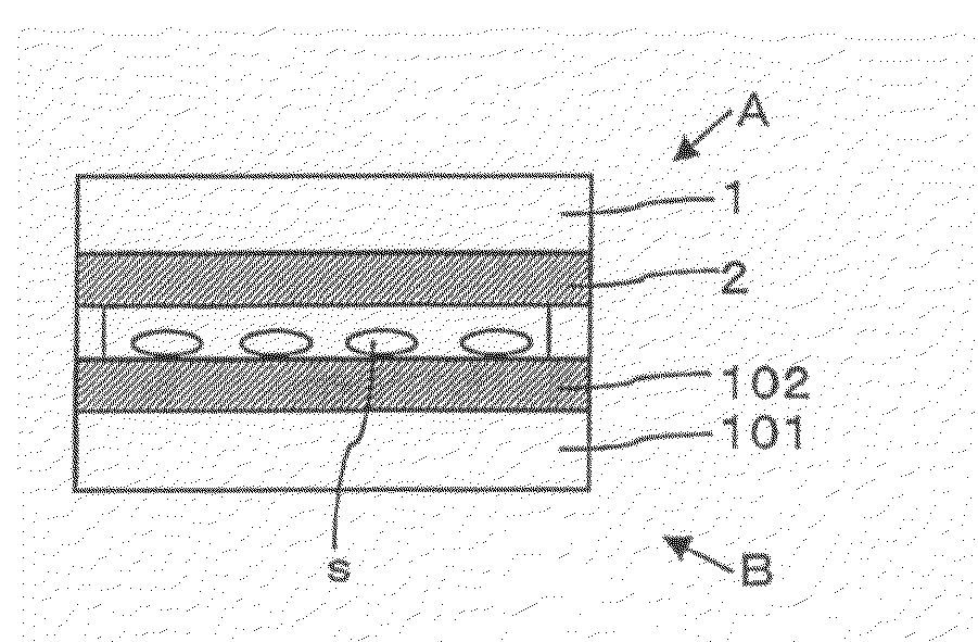
[0088]A cured film having a thickness of 150 nm made of a thermosetting resin where melamine resin:alkyd resin:organic silane condensate=2:2:1 (weight ratio) was formed on one surface of a first transparent film base made of a polyethylene terephthalate film (hereinafter, referred to as PET film) having a thickness of 23 μm through gravure coating (shown as Si coating in Table 1). This is referred to as first transparent dielectric thin film.

[0089]Next, an SiO2 film having a thickness of 30 nm was formed on the above described first dielectric thin film in accordance with a vacuum vapor deposition method. This is referred to as second transparent dielectric thin film.

[0090]Furthermore, a transparent conductive thin film (ITO thin film) having a thickness of 23 nm was formed from a composite oxide of indium oxide and tin oxide on the above described second dielectric thin film in accordance with a sputtering method using a sintered body of a mixture of ...

example of manufacture 2

(Fabrication of First Panel A2)

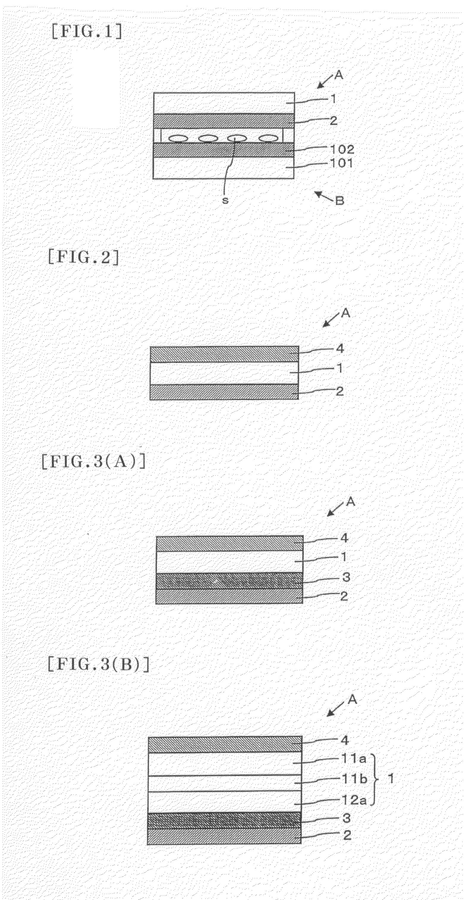
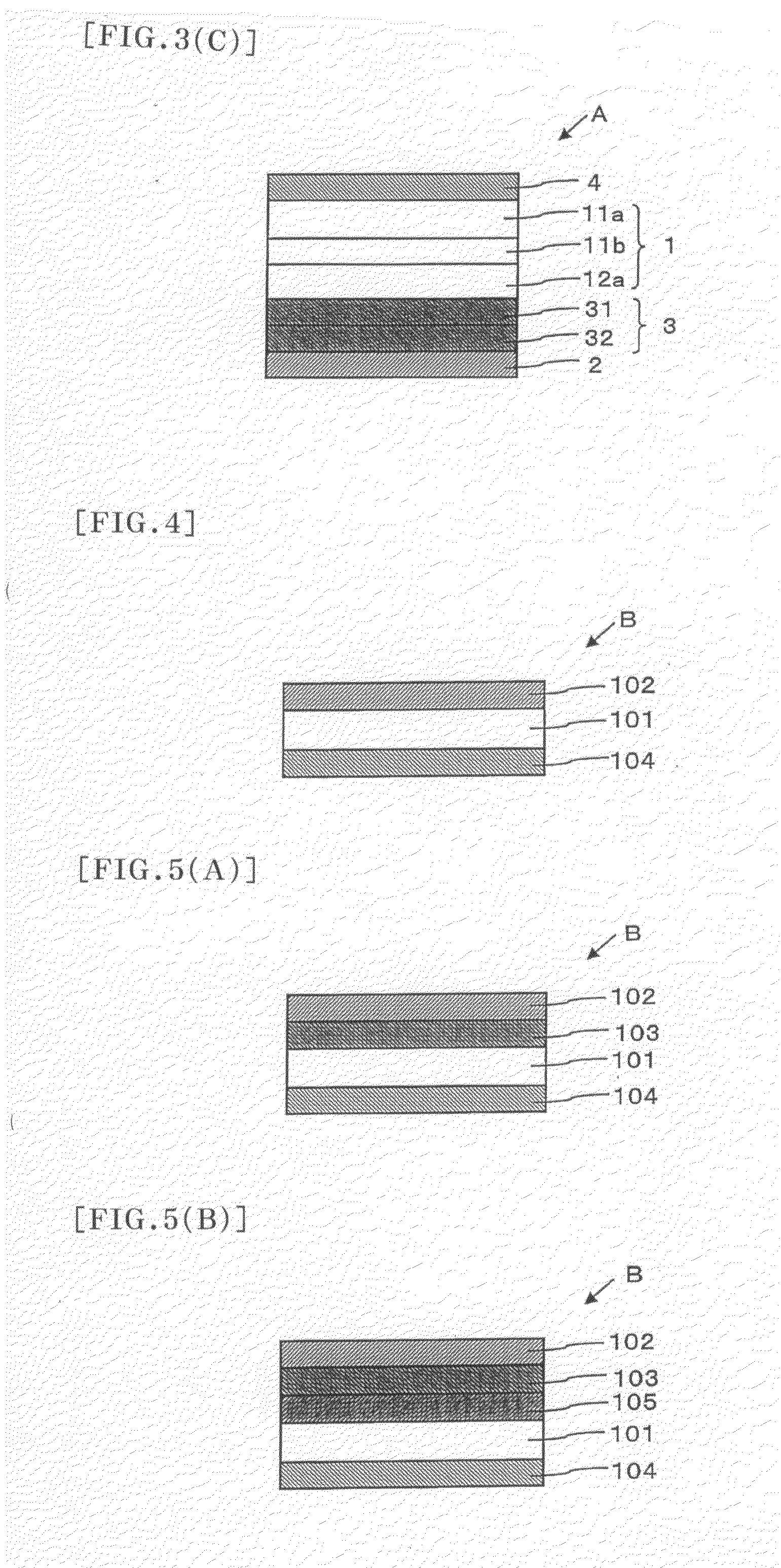
[0093]A first panel A2 was fabricated in the same manner in Example of Manufacture 1, except that the thickness of the SiO2 film was changed to 70 nm as in Example of manufacture 1.


PUM


Abstract

A touch panel of the invention comprises a first panel having a first film base with transparency and a first transparent conductive thin film provided on one surface of the first film base; and a second panel having a second film base with transparency and a second transparent conductive thin film provided on one surface of the second film base, wherein the first panel and the second panel are arranged so as to face each other with a spacer therebetween, in such a manner that the first conductive thin film and the second conductive thin film face each other, wherein the surface of the first conductive thin film has a hardness of 1 GPa or more and a modulus of elasticity of 5 GPa or more, the surface of the second conductive thin film has a center line average roughness (Ra) of 0.3 nm to 1.0 nm, and that of the center line average roughness (Ra) of the surface of the second conductive thin film is smaller than that of the surface of the first conductive thin film. The touch panel has good durability.

Description

BACKGROUND OF THE INVENTION[0001]1. Field of the Invention[0002]The present invention relates to a touch panel where panels having a conductive thin film provided on a film base are used as upper and lower substrates.[0003]2. Description of the Related Art[0004]Touch panels where bases on which transparent conductive thin films are provided are placed so as to face each other with spacers therebetween are used in such a manner that the above described conductive thin films are used as transparent electrodes. Though conventionally, so-called conductive glass where an indium oxide thin film is formed on a glass as well known for conductive thin films as that described above, it is inferior in terms of flexibility and processability, because the base is a glass, and therefore, it cannot be used for some applications.[0005]Therefore, in recent years, conductive thin films where a variety of plastic films, including polyethylene terephthalate films, are used as the base have been used, b...

Claims


Application Information

Patent Timeline
Patent Type & Authority Applications(United States)
IPC IPC(8): G06F3/041
CPCG06F3/045H01H2201/00H01H2201/016H01H2227/002H01H2227/004H01H2227/006Y10T428/24355H01H2227/01H01H2227/03H01H2227/034H01H13/704Y10T428/24372H01H2227/008
Inventor NASHIKI, TOMOTAKESUGAWARA, HIDEO
Owner NITTO DENKO CORP
Why Eureka
Try Eureka