

Structure, transmission type liquid crystal display, reflection type display and manufacturing method thereof
a technology of liquid crystal display and transmission type, applied in non-linear optics, instruments, optics, etc., can solve the problems of low yield, difficulty in achieving high accuracy, cost rise,
- Summary
- Abstract
- Description
- Claims
- Application Information
AI Technical Summary
Problems solved by technology
Method used
Image

Examples
example 1
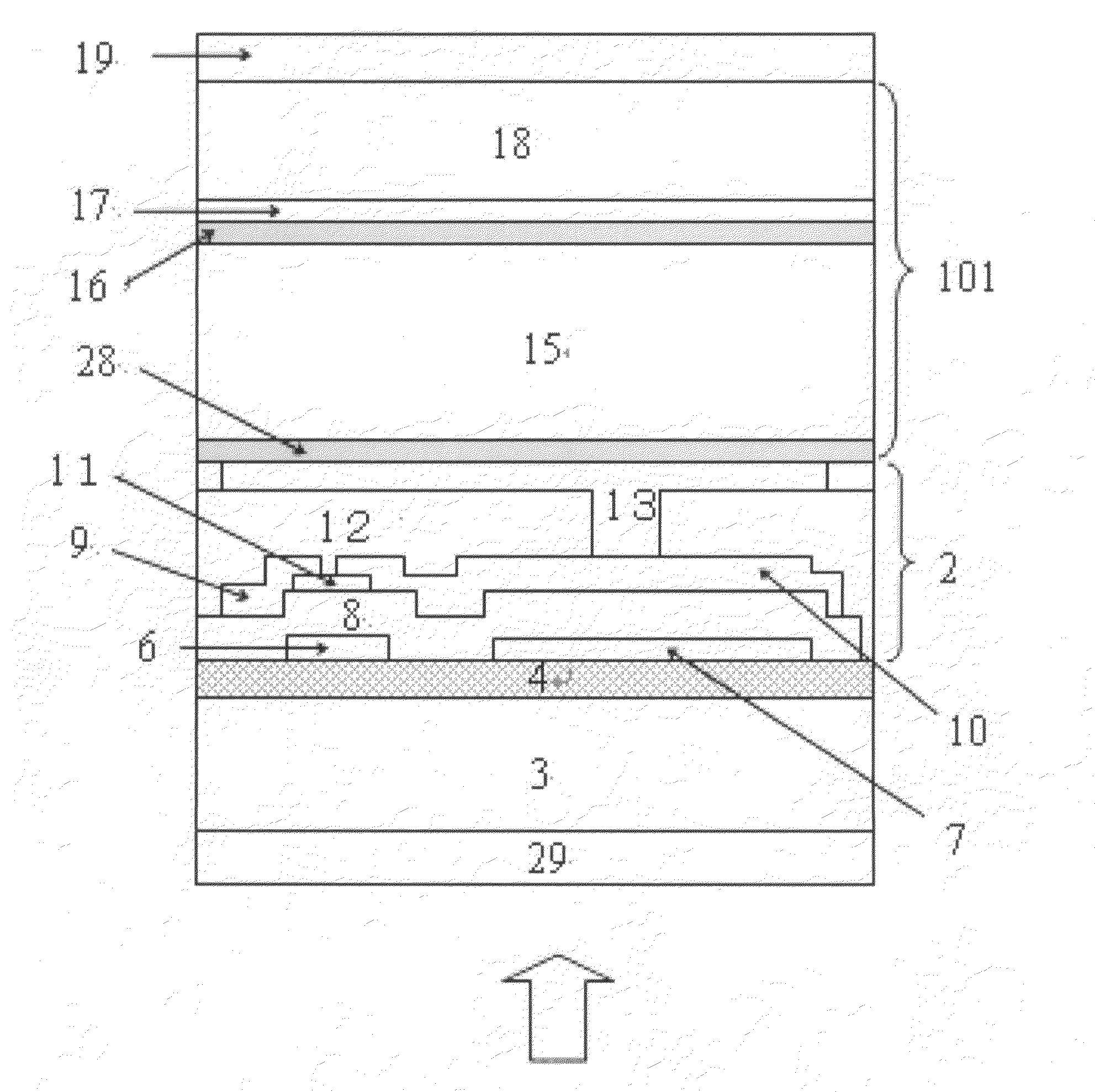
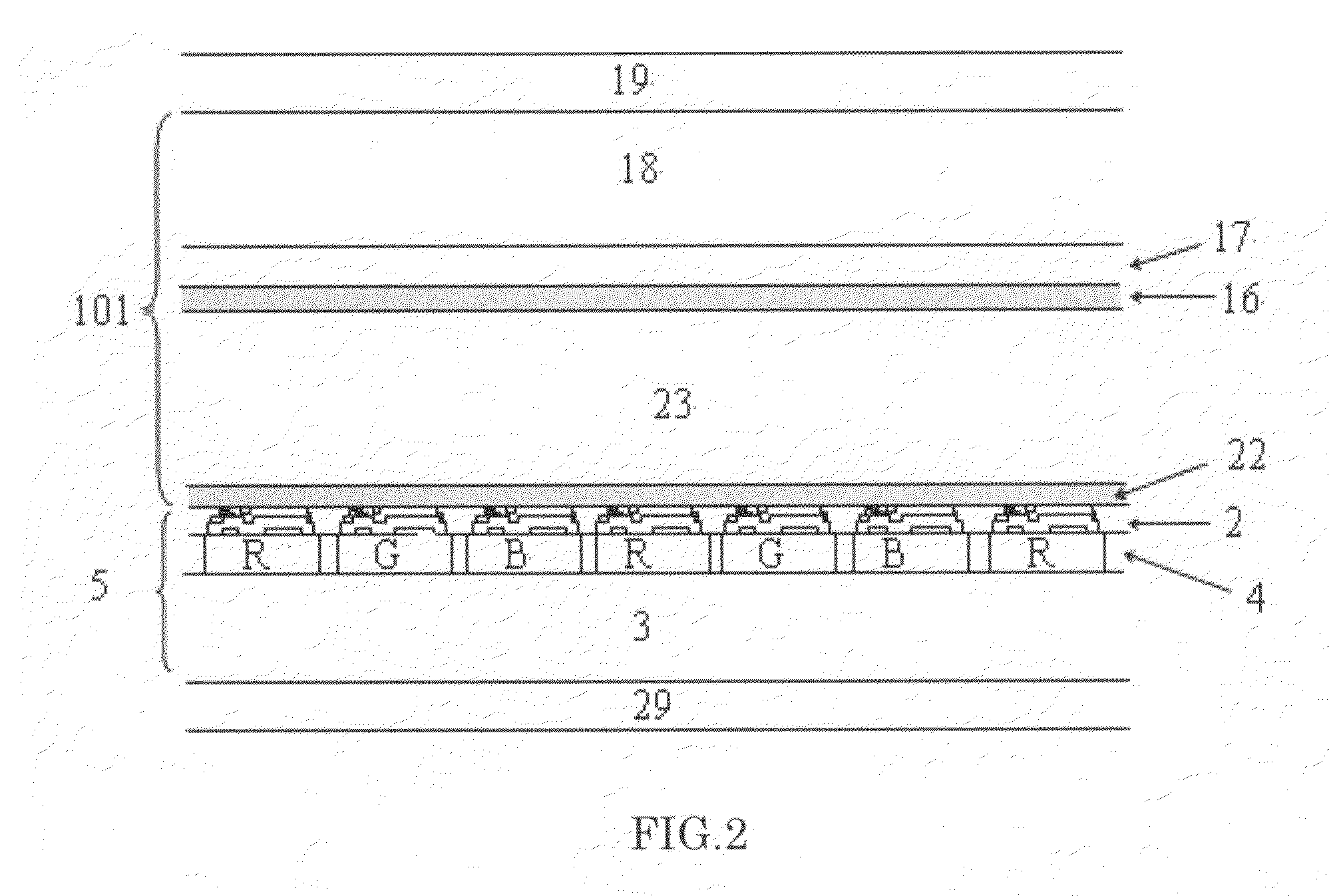
[0088]Sectional drawings of example 1 are shown in FIG. 1 and FIG. 2. FIG. 1 is a partial cross section for approximately 1 pixel of a transmission type display of an example of the present invention. FIG. 2 is a section view of a transmission type liquid crystal display of an example of the present invention.
[0089]For substantially transparent plate substrate 3, alkali-free glass 1737 (thickness 0.5 mm) made in Corning were used. Color filter layer 4 comprising R (red), G (green) and B (blue) was formed on one side of the substrate. Thereupon, a protective layer comprising a transparent resin was formed.
[0090]Then, ITO thin film of 50 nm thickness was formed over color filter layer 4 by DC magnetron sputtering technique. And, the ITO thin film was patterned into a desired shape while position adjustment between the patterned ITO thin film and a color filter layer was performed. In this way, gate electrode 6 and auxiliary capacitor electrode 7 were formed.
[0091]Further, using a targ...
example 2
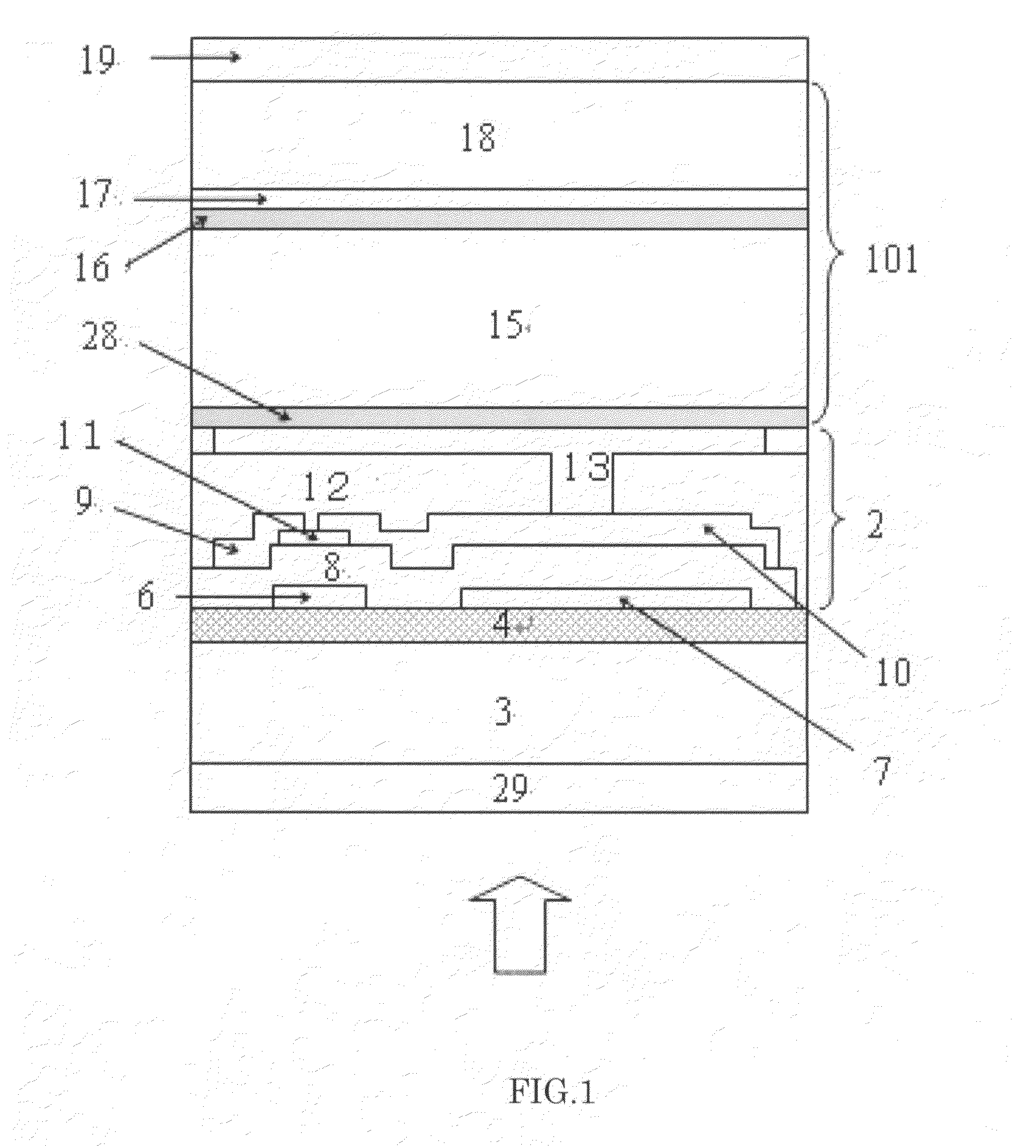
[0101]Sectional drawings of an example are shown in FIG. 1 and FIG. 2. FIG. 1 is a partial cross section for approximately 1 pixel of a transmission type display of an example of the present invention. FIG. 2 is a section view of a transmission type liquid crystal display of an example of the present invention.
[0102]For substantially transparent plate substrate 3, alkali-free glass 1737 (thickness 0.5 mm) made in Corning were used. Color filter layer 4 comprising R (red), G (green) and B (blue) was formed on one side of the substrate. Thereupon, a protective layer comprising a transparent resin was formed.
[0103]Then, ITO thin film of 50 nm thickness was formed over color filter layer 4 by DC magnetron sputtering technique. And, the ITO thin film was patterned into a desired shape while position adjustment between the patterned ITO thin film and a color filter layer was performed. In this way, gate electrode 6 and auxiliary capacitor electrode 7 were formed.
[0104]Further, using a tar...
example 3
[0115]Sectional drawings of an example are shown in FIG. 3 and FIG. 4. FIG. 3 is a partial cross section for approximately 1 pixel of a reflection type display of an example of the present invention. FIG. 4 is a section view of a reflection type display of an example of the present invention.
[0116]For substantially transparent plate substrate 3, alkali-free glass 1737 (thickness 0.7 mm) made in Corning were used.
[0117]At first, by a spin coat of a red photosensitive coloring composition, a red colored layer was obtained on a substrate. Next, through a photo mask, ultraviolet irradiation of 100 mJ / cm2 was performed using an ultra-high pressure mercury lamp. After ultraviolet irradiation, this substrate was soaked in 0.5% sodium carbonate solution for one minute.
[0118]Subsequently, by using ion exchanged water, this substrate was washed with water for 30 seconds. This substrate was heat-treated for 20 minutes at 230 degrees Celsius. Red pattern was formed in this way.
[0119]Spin coat o...
PUM
 Abstract
Description
Claims
Application Information