CATALYST-FREE GROWTH OF GaN NANOSCALE NEEDLES AND APPLICATION IN InGaN/GaN VISIBLE LEDS

a nano-scale needle and catalyst-free technology, applied in the direction of crystal growth process, polycrystalline material growth, instruments, etc., can solve the problems of catalyst being inevitably incorporated into the nano-needle, degrading the crystalline quality, and the catalytic process cannot control the position and uniformity of the nano-needl

Inactive Publication Date: 2007-11-08
RGT UNIVESITY OF NEW MEXICO
View PDF4 Cites 82 Cited by
  • Summary
  • Abstract
  • Description
  • Claims
  • Application Information

AI Technical Summary

Benefits of technology

[0007] According to various embodiments, the present teachings include a method of making nanoneedles. In the method, a growth mask layer can be formed over a buffer layer formed over a semiconductor substrate. A plurality of patterned apertures can be formed through the growth mask layer to expose a plurality of portions of ...

Problems solved by technology

Problems arise, however, because these conventional catalytic processes cannot control the position and uniformity of the resulting nanoneedles.
A further problem with conventional cat...

Method used


Image

  • CATALYST-FREE GROWTH OF GaN NANOSCALE NEEDLES AND APPLICATION IN InGaN/GaN VISIBLE LEDS
  • CATALYST-FREE GROWTH OF GaN NANOSCALE NEEDLES AND APPLICATION IN InGaN/GaN VISIBLE LEDS
  • CATALYST-FREE GROWTH OF GaN NANOSCALE NEEDLES AND APPLICATION IN InGaN/GaN VISIBLE LEDS

Examples


Embodiment Construction

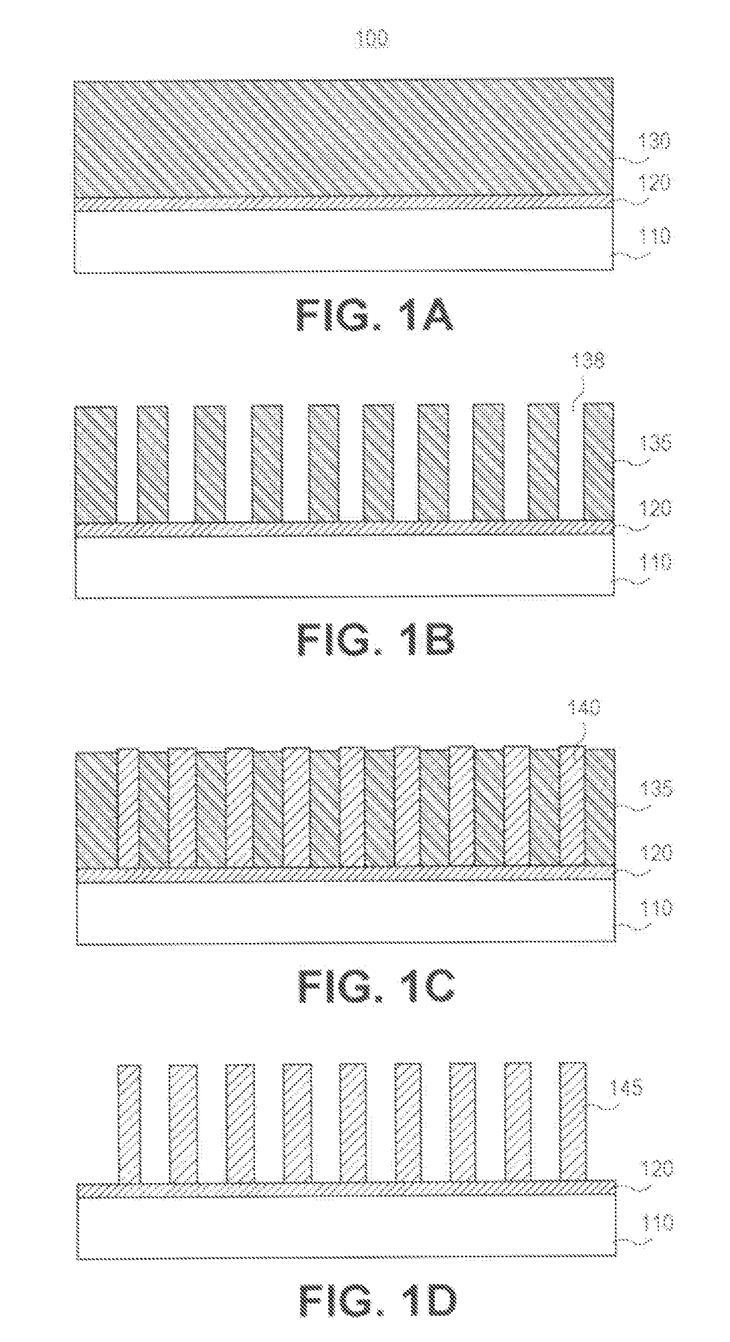
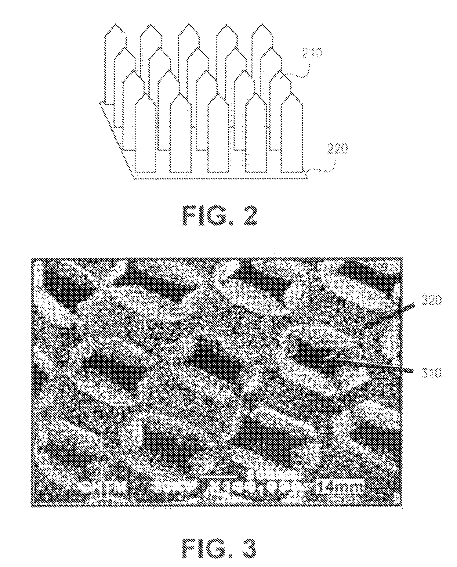
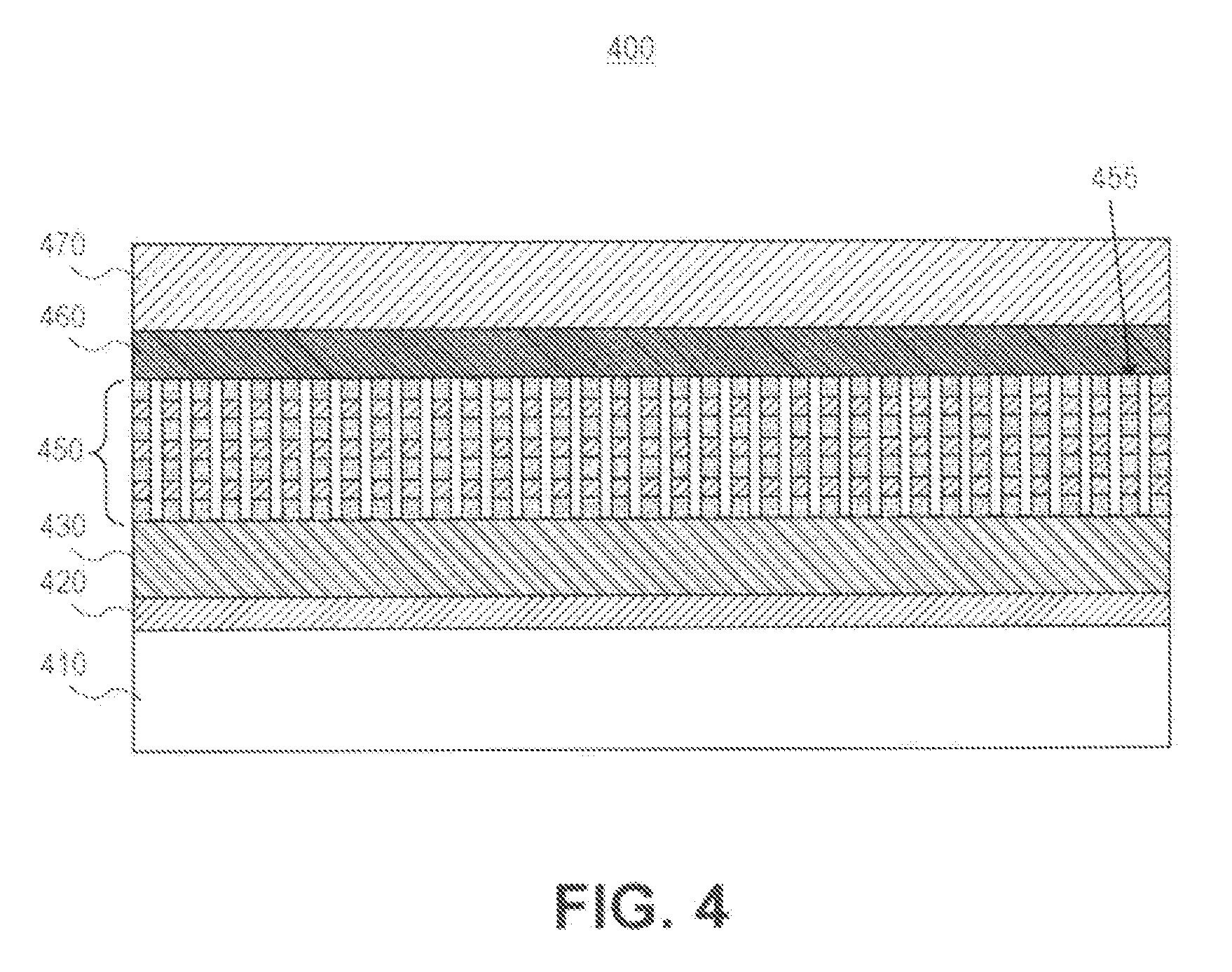
[0019] Reference will now be made in detail to exemplary embodiments of the invention, an example of which is illustrated in the accompanying drawings. Wherever possible, the same reference numbers will be used throughout the drawings to refer to the same or like parts. In the following description, reference is made to the accompanying drawings that form a part thereof, and in which is shown by way of illustration specific exemplary embodiments in which the invention may be practiced. These embodiments are described in sufficient detail to enable those skilled in the art to practice the invention and it is to be understood that other embodiments may be utilized and that changes may be made without departing from the scope of the invention. The following description is, therefore, merely exemplary.

[0020] While the invention has been illustrated with respect to one or more implementations, alterations and / or modifications can be made to the illustrated examples without departing fro...


PUM


Abstract

Exemplary embodiments provide a scalable process for the growth of large scale and uniform III-N nanoneedle arrays with precise control of the position, cross sectional shape and/or dimensions for each nanoneedle. In an exemplary process, a plurality of nanoneedle array can be formed by growing one or more semiconductor material in a plurality of patterned rows of apertures with a predetermined geometry. The plurality of patterned rows of apertures can be formed though a thick selective nanoscale growth mask, which can later be removed to expose the plurality of nanoneedle arrays. The plurality of nanoneedle arrays can be connected top and bottom by a continuous coalesced epitaxial film, which can be used in a planar semiconductor process or be further configured as a photonic crystal to improve the output coupling of nanoscale optoelectronic devices such as LEDs and/or lasers.

Description

RELATED APPLICATIONS [0001] This application claims priority from U.S. Provisional Patent Application Ser. No. 60 / 735,198, filed Nov. 10, 2005, which is hereby incorporated by reference in its entirety.FIELD OF THE INVENTION [0002] This invention relates generally to light emitting diodes (LEDs), and, more particularly, to LEDs that include nanoneedle arrays. BACKGROUND OF THE INVENTION [0003] Nanoscale needles, also referred to herein as nanowires, composed of group III-N alloys (e.g., GaN) provide the potential for new semiconductor device configurations such as nanoscale optoelectronic devices. If this potential is to be fully realized, a scalable process is required to form high quality group III-N nanoneedles with precise control of the geometry and position of each nanoneedle. [0004] Conventional nanoneedle preparation is based on the vapor-liquid-solid (VLS) growth mechanism and involves the use of catalysts such as Au, Ni, Fe, or In. Problems arise, however, because these co...

Claims


Application Information

Patent Timeline
IPC IPC(8): H01L33/00H01L31/0256H01L33/08
CPCB82Y20/00H01L2933/0083C30B25/00C30B29/60G02B6/107H01L21/0237H01L21/02458H01L21/02521H01L21/0254H01L21/02603H01L21/02639H01L21/02642H01L21/0265H01L21/02664H01L33/007H01L33/08C30B23/00
Inventor HERSEE, STEPHEN D.WANG, XINBRUECK, STEVEN R.J.SUN, XINYU
Owner RGT UNIVESITY OF NEW MEXICO
Why Eureka
Try Eureka