Method and apparatus for photo-excitation of chemicals for atomic layer deposition of dielectric film

a dielectric film and chemical technology, applied in the field of chemical vapor deposition process and atomic layer deposition process, can solve the problems of increasing affecting the number of substrates, and challenging to provide processing conditions uniformly over an increased number of substrates,

Inactive Publication Date: 2007-11-08
APPLIED MATERIALS INC
View PDF99 Cites 55 Cited by
  • Summary
  • Abstract
  • Description
  • Claims
  • Application Information

AI Technical Summary

Benefits of technology

[0013]According to another embodiment, a method for forming a metal layer on a substrate is provided. The method comprises positioning a substrate within a process chamber, exposing the substrate to a deposition gas comprising a metal containing precursor and a reducing gas, exposing the deposition gas to an energy beam derived from a UV-sou

Problems solved by technology

The COO, while affected by a number of factors, is greatly affected by the number of substrates processed per time, i.e., the throughput of the fabrication process, and cost of processing materials.
However, providing processing conditions uniformly over an increased number of substrates is a challenging task.
Providing uniform process conditions over an increased number of substrates is

Method used


Image

  • Method and apparatus for photo-excitation of chemicals for atomic layer deposition of dielectric film
  • Method and apparatus for photo-excitation of chemicals for atomic layer deposition of dielectric film
  • Method and apparatus for photo-excitation of chemicals for atomic layer deposition of dielectric film

Examples


Embodiment Construction

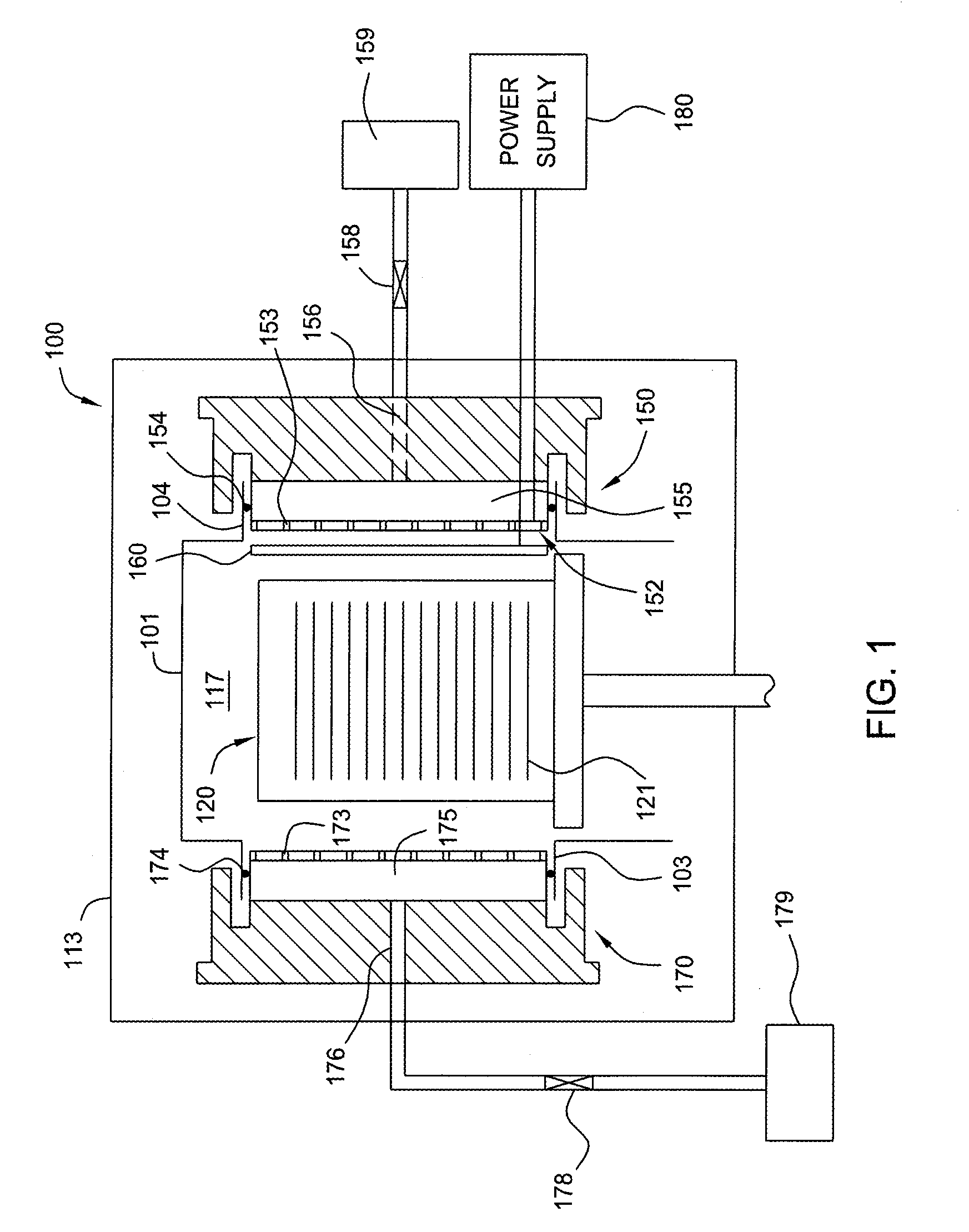
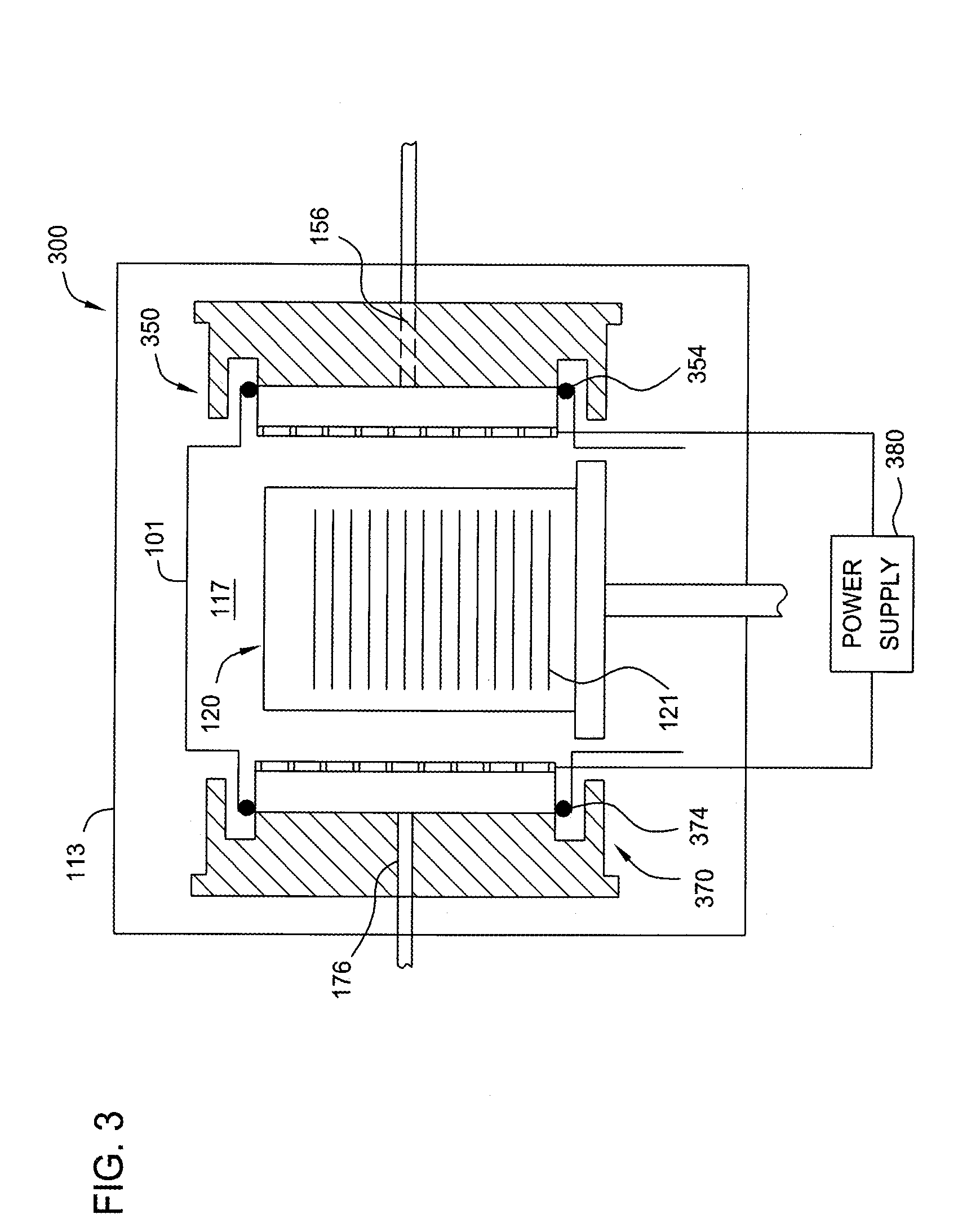
[0029]The invention generally provides an apparatus and a method for processing semiconductor substrates in a batch with assemblies for assisting the processes by generated ions. In one embodiment of the invention, a batch processing chamber with an excitation assembly, which is positioned within the batch processing chamber housing, is provided. An example of a batch processing chamber which may be useful for one embodiment described herein is a FLEXSTAR® system, available from Applied Materials, Inc., located in Santa Clara, Calif.

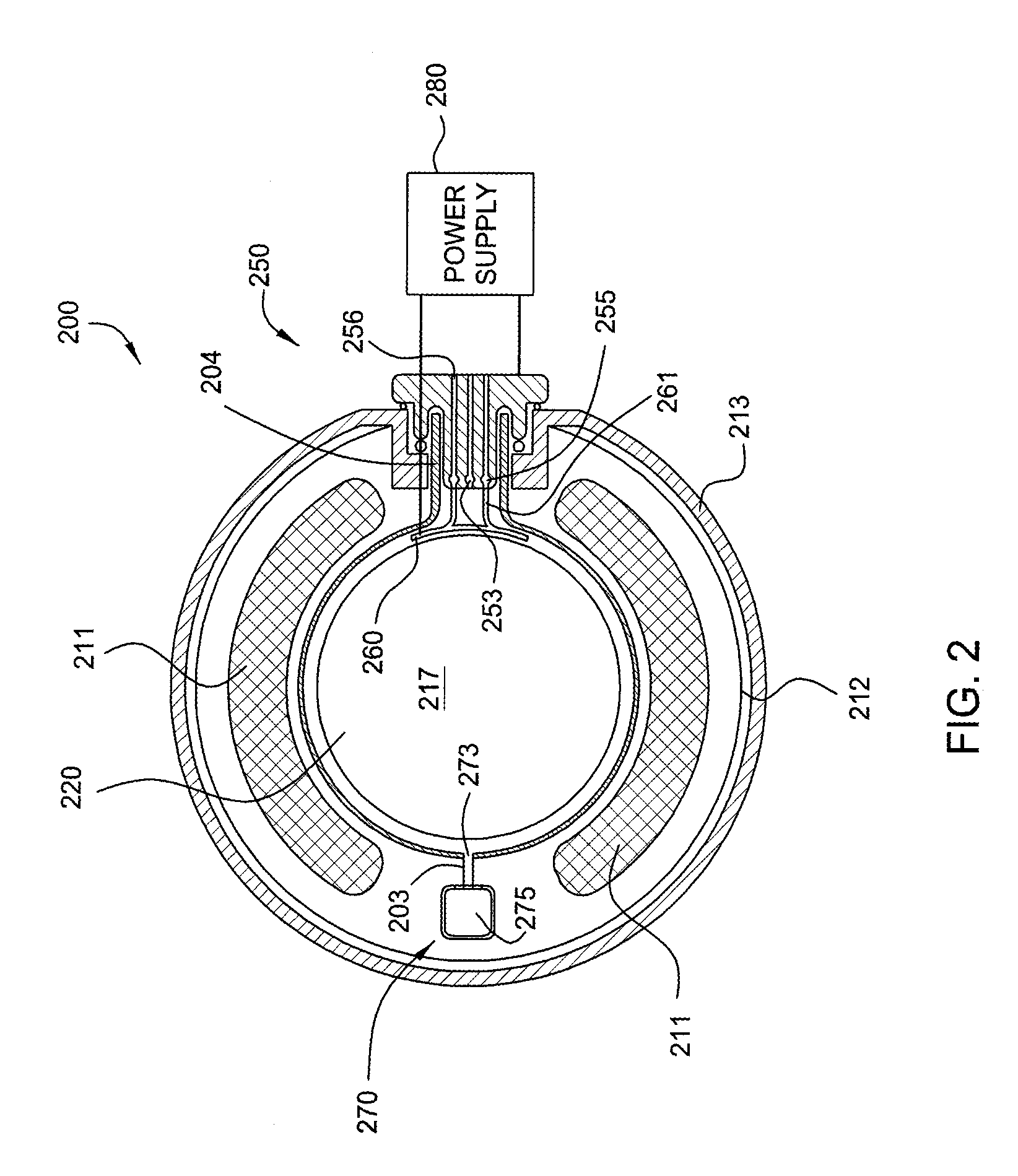
[0030]Generally, excited species of processing gases may be generated to assist the ALD or CVD processes as described herein. These species may be excited by plasma assistance, UV assistance (photo assistance), ion assistance (e.g., ions generated by an ion source), or combinations thereof. The species are excited in or in the vicinity of the process region within the chamber housing to avoid relaxation of the excited states before the ions reach the pro...


PUM

PropertyMeasurementUnit
Energyaaaaaaaaaa
Energyaaaaaaaaaa
Energyaaaaaaaaaa

Abstract

The invention generally provides a method for depositing materials, and more particularly, embodiments of the invention relate to chemical vapor deposition processes and atomic layer deposition processes utilizing photoexcitation techniques to deposit barrier layers, seed layers, conductive materials, and dielectric materials. Embodiments of the invention generally provide methods of the assisted processes and apparatuses, in which the assisted processes may be conducted for providing uniformly deposited material.

Description

CROSS-REFERENCE TO RELATED APPLICATIONS[0001]This application is a continuation-in-part of co-pending U.S. patent application Ser. No. 11 / 381,970 (APPM / 010749), filed May 5, 2006, which is herein incorporated by reference.BACKGROUND OF THE INVENTION[0002]1. Field of the Invention[0003]Embodiments of the invention generally relate to a method for depositing materials, and more particularly, embodiments of the invention relate to chemical vapor deposition processes and atomic layer deposition processes utilizing photoexcitation techniques to deposit barrier layers, seed layers, conductive materials, and dielectric materials.[0004]2. Description of the Related Art[0005]A substrate fabrication process is often evaluated by two related and important factors, which are device yield and the cost of ownership (COO). The COO, while affected by a number of factors, is greatly affected by the number of substrates processed per time, i.e., the throughput of the fabrication process, and cost of ...

Claims


Application Information

Patent Timeline
IPC IPC(8): C23C16/00
CPCC23C16/45508C23C16/45574H01J37/32009C23C16/46C23C16/509C23C16/4583C23C16/0209C23C16/0245C23C16/045C23C16/34C23C16/403C23C16/405C23C16/4405C23C16/45504C23C16/45591C23C16/482H01L21/205C23C16/00H05H1/24
Inventor SINGH, KAUSHAL K.MAHAJANI, MAITREYEEGHANAYEM, STEVE G.YUDOVSKY, JOSEPHMCDOUGALL, BRENDAN
Owner APPLIED MATERIALS INC
Why Eureka
Try Eureka