Semiconductor device and wiring auxiliary pattern generating method

a technology of auxiliary pattern and semiconductor device, which is applied in the direction of semiconductor device, semiconductor/solid-state device details, electrical apparatus, etc., can solve the problems of inability to dispose of dummy wiring, inability to provide dummy wiring and dummy via, and thin interlayer insulating film, etc., and achieve low probability of generating inconvenience such as under-etching and connection failur

Inactive Publication Date: 2007-11-15
PANASONIC CORP
View PDF8 Cites 38 Cited by
  • Summary
  • Abstract
  • Description
  • Claims
  • Application Information

AI Technical Summary

Benefits of technology

[0024] When it is judged in the step (i) that the sum of the via patterns and the dummy via patterns is larger than the fourth prescribed value, dummy pattern modules distant from the via patterns are eliminated in the step (j), among the dummy pattern modules disposed within the area that is extracted in the step (c). This makes it possible to securely prevent the inconveniences such as short-circuits generated between the wirings due to the metal that is remained on the interlayer insulating film because of under-etching, at least in the areas close to the via patterns.
[0025] When it is judged in the step (i) that the sum of the via patterns and the dummy via patterns is larger than the fourth prescribed value, the dummy pattern modules connected to the first wiring patterns disposed on every other wiring grid lines and the dummy pattern modules connected to the second wiring patterns disposed on every other wiring grid lines are eliminated in the step(j). This expands the space between the dummy via patterns, so that generation of inconveniences such as short-circuits between the wirings or between the wirings and the dummy wirings can be suppressed during the actual manufacturing steps of the semiconductor device.
[0026] As described above, the wiring auxiliary pattern generating method of the present invention disposes the dummy via pattern that is only connected either to the first wiring pattern or to the second wiring pattern. Thus, the dummy via pattern can be disposed even in the area where the wirings are densely provided. As a result, it becomes possible to set the sum of the via patterns and the dummy via patterns within a prescribed area to be in a proper range.
[0027] Furthermore, in the semiconductor device to which the wiring auxiliary pattern of the present invention is applied, the sum of the vias and the dummy vias within a prescribed range is set to be within a proper range. Therefore, probability of generating inconveniences such as under-etching and connection failure can be suppressed low.

Problems solved by technology

Thus, the dummy wirings and the dummy vias cannot be provided in an area with highly dense wirings of a highly integrated and highly dense integrated circuit such as a system LSI.
Further, in the case where the dummy wirings and the dummy vias are electrically connected to the power supply wiring and the ground wiring, it is not possible to dispose the dummy wirings and the dummy vias in an area where there is no power supply wiring and ground wiring in the periphery of the dummy wirings and the dummy vias.
This causes an over-etching, for example, so that there are generated such inconveniences that the interlayer insulating film becomes thin, and the via hole become shallow.
Thus, there may be cases where residual substances remain in the via holes.
In such a case, the via hole connecting between the lower layer wiring and the upper layer wiring cannot be filled with a metal, so that it is possible generate such an inconvenience that the wiring is cut in this area, etc.

Method used


Image

  • Semiconductor device and wiring auxiliary pattern generating method
  • Semiconductor device and wiring auxiliary pattern generating method
  • Semiconductor device and wiring auxiliary pattern generating method

Examples


first embodiment

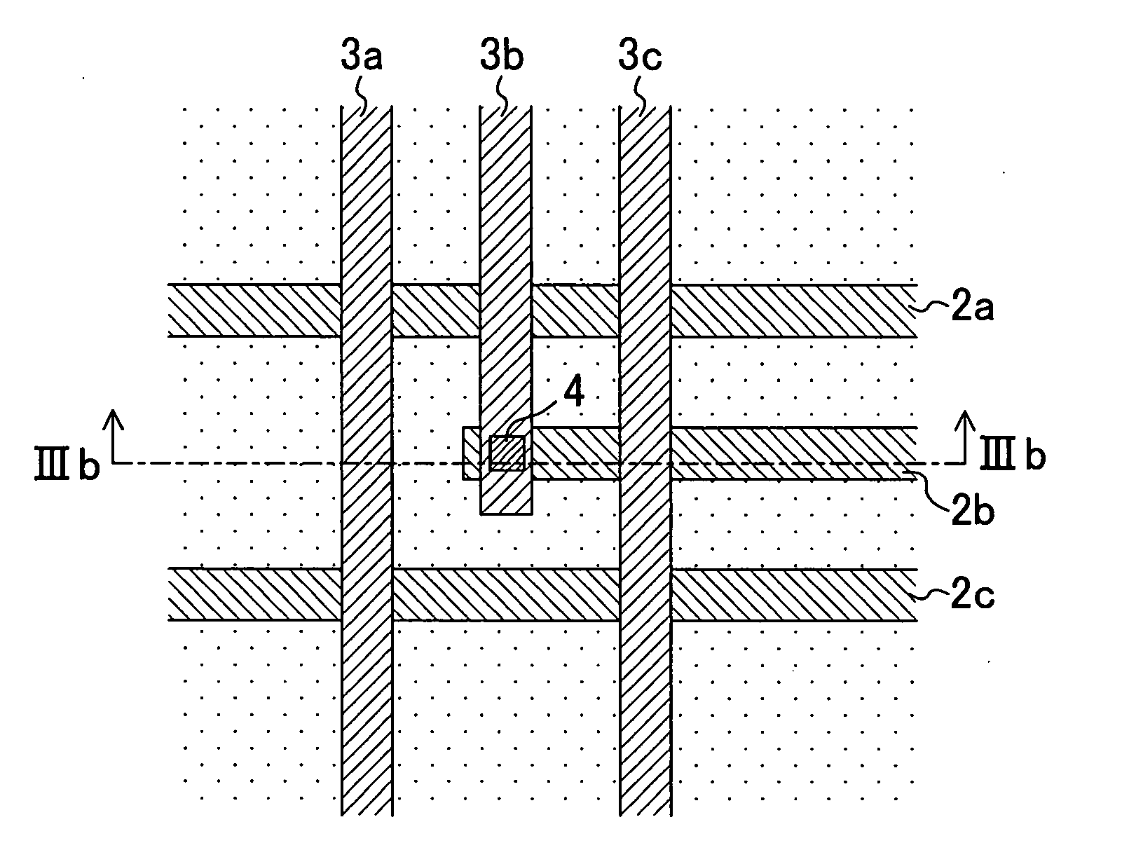
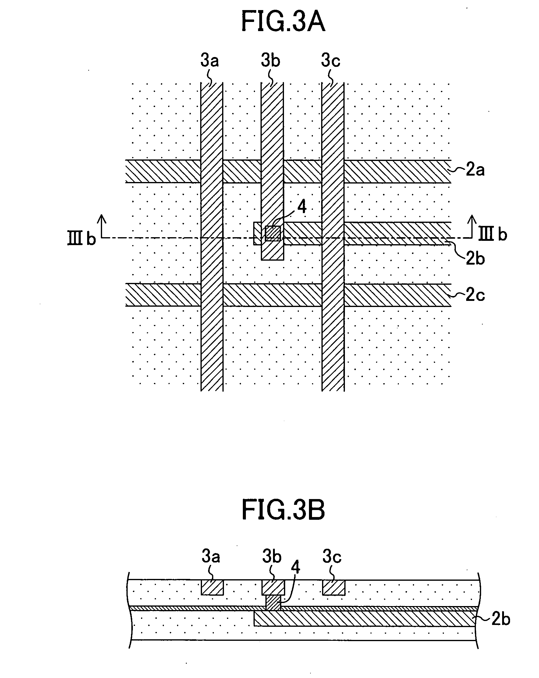
[0051]FIG. 1 is a flowchart for illustrating a wiring auxiliary pattern generating method according to a first embodiment of the present invention, and FIG. 2 is a flowchart for illustrating in detail a part of the steps in the wiring auxiliary pattern generating method according to the first embodiment. Further, FIG. 3A is a plan view for showing a wiring layout when a semiconductor integrated circuit is viewed above, and FIG. 3B is a sectional view of the semiconductor integrated circuit taken along the line IIIb-IIIb of FIG. 3A. FIG. 4A is a plan view for showing a wiring layout when a semiconductor integrated circuit to which the wiring auxiliary pattern generating method according to the first embodiment is applied is viewed from above, and FIG. 4B is a sectional view of the semiconductor integrated circuit taken along the line IVb-IVb of FIG. 4A. FIGS. 5A -5J are diagrams for describing the procedure for applying the wiring auxiliary pattern generating method according to the ...

second embodiment

[0076]FIG. 7 is a flowchart for illustrating the dummy pattern module generating method according to a second embodiment of the present invention. FIG. 8 is a flowchart for illustrating in detail the steps shown in FIG. 7 in the wiring auxiliary pattern generating method according to the second embodiment. FIGS. 9A and 9B are plan views for describing the wiring auxiliary pattern generating method of this embodiment, which illustrate examples of the actual pattern. FIG. 5 is used for describing the wiring auxiliary pattern generating method of this embodiment.

[0077] The wiring auxiliary pattern of this embodiment is generated in the following manner.

[0078] First, as shown in FIG. 7, the steps s101-s104 are carried out. In the step s104, the dummy pattern modules 19a-19k shown in FIG. 5J are outputted.

[0079] Then, among the dummy pattern modules generated in the step s104, dummy pattern modules connected to a part of the wiring patterns are eliminated in a step s301. Specifically,...

third embodiment

[0087]FIG. 10 is a flowchart for illustrating the wiring auxiliary pattern generating method according to a third embodiment of the present invention. FIGS. 11A and 11B are plan views for describing the wiring auxiliary pattern generating method according to the third embodiment, which respectively illustrate actual pattern examples. FIG. 5, which is referred to in describing the first embodiment, is used for describing the wiring auxiliary pattern generating method of this embodiment.

[0088] The wiring auxiliary pattern of this embodiment is generated in the following manner.

[0089] First, the steps s101-s104 and the step s301 shown in FIG. 10 are carried out. The steps s101-s104 are the same steps as those described in the first embodiment, and the step s301 is the same step as that described in the second embodiment. That is, the dummy pattern modules 19a-19k shown in FIG. 5J are outputted in the step s104, and dummy pattern modules 19d, 19e among the dummy pattern modules 19a-19...


PUM


Abstract

An area with a low via pattern density is extracted from a semiconductor integrated circuit that includes the first wirings and the second wirings disposed on the upper layer of the first wirings, based on wiring layout information. Then, dummy via patterns connected either to the first wirings or the second wirings are disposed in the peripheral area of the via patterns within the selected area. With this, the dummy via can be disposed even in an area where the wirings are congested.

Description

BACKGROUND OF THE INVENTION [0001] 1. Technical Field [0002] The present invention relates to a semiconductor device, and more particularly, to an LSI wiring structure that comprises dummy vias and dummy wirings. [0003] 2. Related Art [0004] In a semiconductor device having multilayer wirings such as a semiconductor integrated circuit, an interlayer insulating film is formed after forming a lower wiring layer, and specific areas of the interlayer insulating film are selectively etched to form via holes thereby to expose the surface of the lower wiring layer. Then, a metal film made of tungsten or the like is formed over the interlayer insulating film including the via holes. Subsequently, the metal film over the interlayer insulating film is removed by CMP (Chemical Mechanical Polishing) method, and an upper wiring layer is formed thereafter. [0005] However, when the areas to be selectively etched (areas where the via holes are formed) are not disposed uniformly over the entire area...

Claims


Application Information

Patent Timeline
Patent Type & Authority Applications(United States)
IPC IPC(8): H01L23/52
CPCH01L23/522H01L2924/0002H01L2924/00
Inventor SHIBATA, HIDENORI
Owner PANASONIC CORP
Why Eureka
Try Eureka