Dielectric substrate for wave guide tube and transmission line transition using the same

a technology of waveguide tube and dielectric substrate, which is applied in the direction of electrical equipment, coupling devices, impedence networks, etc., can solve the problems of degrading the performance of the waveguide tube, and achieve good performance and mechanical strength

Inactive Publication Date: 2007-11-15
DENSO CORP
View PDF7 Cites 41 Cited by
  • Summary
  • Abstract
  • Description
  • Claims
  • Application Information

AI Technical Summary

Benefits of technology

[0010]Therefore, a waveguide tube of good performance and mechanical strength can be provided without any additional step.

Problems solved by technology

However, it is difficult to form a flat conductive film due to the surface tension thereof as shown in FIG. 8. further, an uneven surface of the conductive film that is formed on the peripheral wall may degrade the performance of the waveguide tube.
However, this distance may also degrade the performance of the waveguide tube.

Method used


Image

  • Dielectric substrate for wave guide tube and transmission line transition using the same
  • Dielectric substrate for wave guide tube and transmission line transition using the same
  • Dielectric substrate for wave guide tube and transmission line transition using the same

Examples


first embodiment

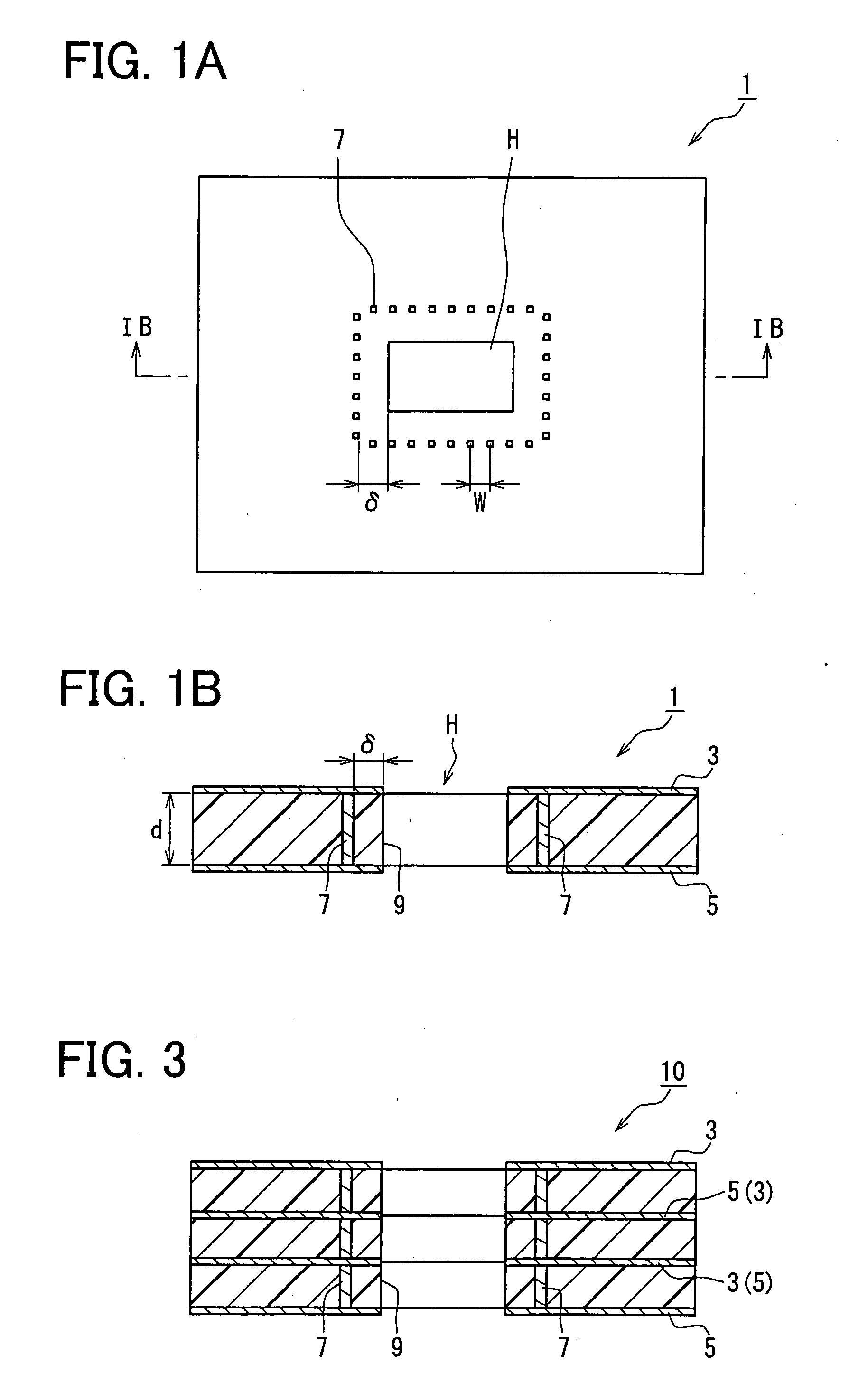
[0024]A dielectric substrate 1 according to the invention will be described with reference to FIGS. 1A and 1B, FIGS. 2A and 2B and FIG. 3.

[0025]The dielectric substrate 1 has conductive layers 3, 5 respectively formed on the upper and lower surfaces thereof, each of which has a ground pattern, a signal line pattern. The dielectric substrate 1 also has a thickness d (e.g. about 100 μm) and a rectangular hole H whose size (e.g. 2.54 mm×1.27 mm) is substantially the same as the hole of a waveguide tube for transmitting electromagnetic wave of a certain frequency band (e.g. 75-110 GHz).

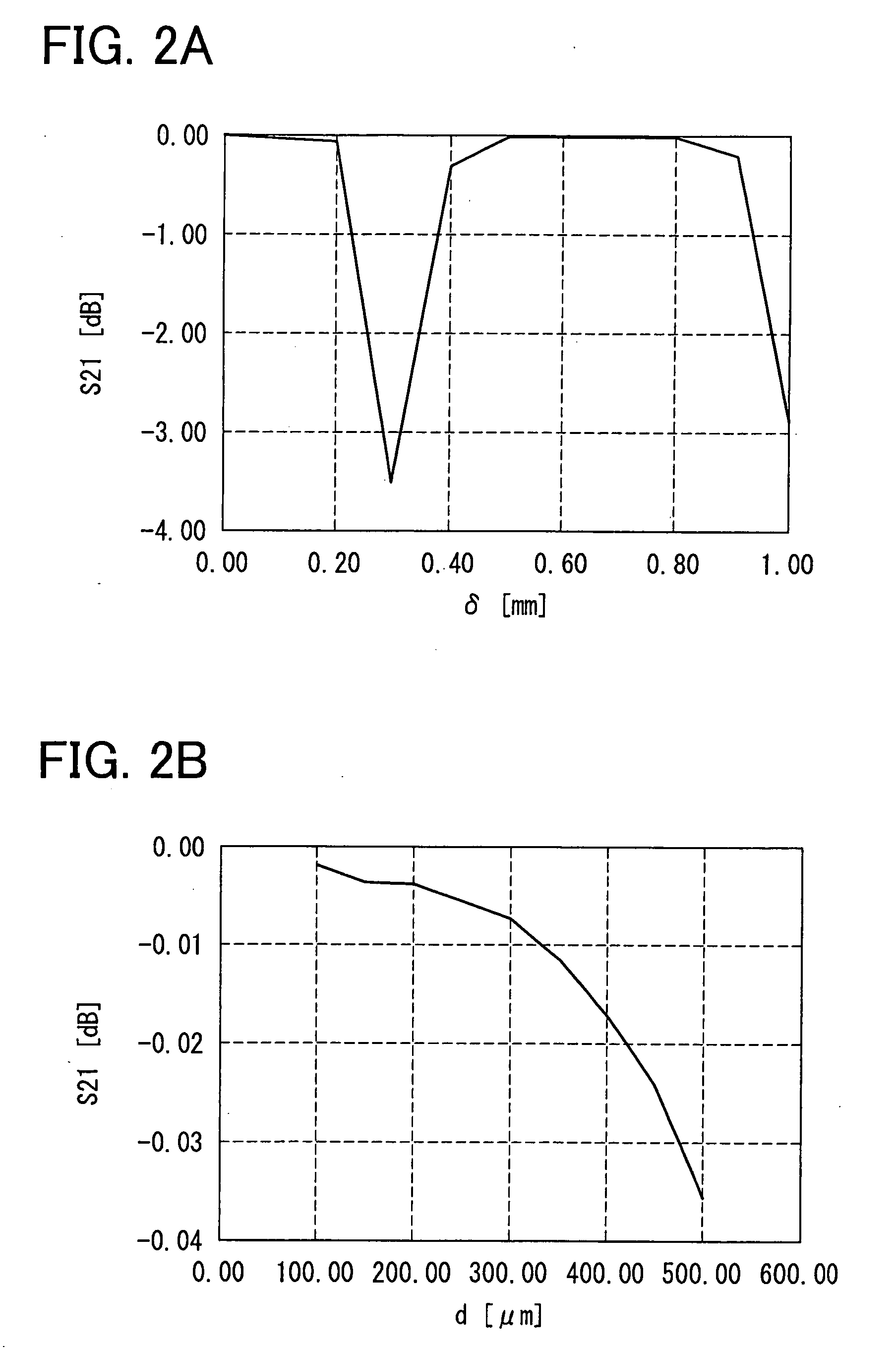
[0026]Plural via holes 7 are formed at equal intervals W in a belt portion of the dielectric substrate 1 at a distance δ from the wall 9 of the hole H. Assuming that the wave length of the transmission signal is λg, the distance δ is designed to be λg / 2 and the interval W is designed to be less than λg / 4. In case of the frequency of the transmission signal being 76.5 GHz, for example, the distance δ is 0....

second embodiment

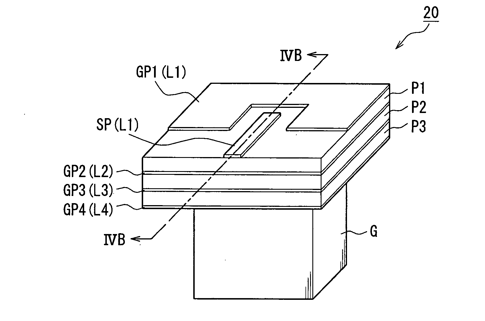
[0032]A transmission line transition 20 according to the invention will be described with reference to FIGS. 4A and 4B and FIG. 5A-5D.

[0033]The transmission line transition 20 is constructed of three dielectric substrates P1-P3 and four pattern layers L1-L4 that are interleaved with each other, so that the dielectric substrate P1 and the pattern layers L1, L2 form a line transition section 20a, and so that the dielectric substrates P2, P3 and the pattern layers L2-L4 form a waveguide tube section 20b.

[0034]The transmission line transition 20 has a rectangular cavity 21 that extends along the center axis of the waveguide tube section 20b to be connected to a waveguide tube G, which is fixed to the waveguide tube section 20b. The waveguide tube G has a rectangular hole of 2.54 mm×1.27 mm to transmit an electromagnetic wave of a frequency between 75 GHz and 110 GHz (e.g. 76.5 GHz).

[0035]The waveguide tube section 20b has plural via holes 23 formed in the dielectric substrates P2, P3 a...

third embodiment

[0042]A transmission line transition 30 according to the invention will be described with reference to FIGS. 6A and 6B.

[0043]The transmission line transition 30 is constructed of three dielectric substrates P1-P3 and four pattern layers L1-L4 that are interleaved with each other, so that the dielectric substrate P1 and the pattern layers L1, L2 form a line transition section 30a, and so that the dielectric substrates P2, P3 and the pattern layers L2-L4 form a waveguide tube section 30b. The waveguide tube section 30b is the same as the waveguide tube section 20b of the second embodiment.

[0044]The line transition section 30a is formed of the dielectric substrate P1 and the pattern layers L1 and L2. The pattern layer L2 has a ground pattern GP2 that covers the entire surfaces of the dielectric substrates P1, P2 confronting each other except for the surface inside the via holes 23. The antenna pattern AP, which is disposed at the bottom of the cavity 21 in the second embodiment, is omi...


PUM


Abstract

A transmission line transition includes a waveguide tube section having a waveguide tube, a waveguide tube section that is formed of at least a dielectric substrate and a line transition section formed of at least a dielectric substrate disposed adjacent the waveguide tube section to cover the hole, a transmission line for transmitting the electromagnetic wave, and an antenna pattern that is disposed in the hole to be electromagnetically coupled with the transmission line. Each of the dielectric substrates has a plurality. of via holes disposed to surround the hole at a distance δ=an integer n×wave length λg / 2 from the peripheral wall of the hole.

Description

CROSS REFERENCE TO RELATED APPLICATION[0001]The present application is based on and claims priority from Japanese Patent Application 2006-134091, filed May 12, 2006, the contents of which are incorporated herein by reference.BACKGROUND OF THE INVENTION[0002]1. Field of the Invention[0003]The present invention relates to a dielectric substrate and a device that utilizes the electric substrate, such as a waveguide or a transmission line transition.[0004]2. Description of the Related Art[0005]Usually, a waveguide tube is formed of plural dielectric substrates each of which has a hole or a cavity. The peripheral wall of the hole is coated with a conductor film, as disclosed in JP-P3347626. When manufacturing a waveguide tube, conductive ink is printed on the peripheral wall to form a conductive film. However, it is difficult to form a flat conductive film due to the surface tension thereof as shown in FIG. 8. further, an uneven surface of the conductive film that is formed on the periph...

Claims


Application Information

Patent Timeline
Patent Type & Authority Applications(United States)
IPC IPC(8): H01P5/107
CPCH01P5/107
Inventor FUJITA, AKIHISA
Owner DENSO CORP
Why Eureka
Try Eureka