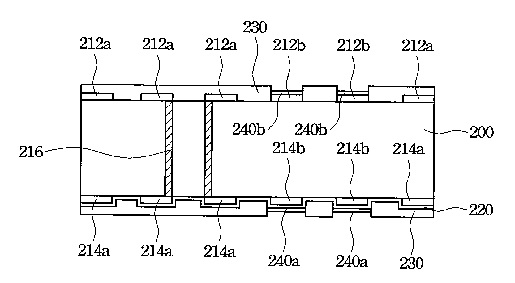
[0017]Reference is made to FIGS. 2A to 2F, which depict cross-sectional diagrams of the process flow in accordance with a preferred embodiment of the present method of manufacturing a substrate for packaging ICs. First of all, a laminated circuit board 200 is provided, which may be a multiplayer circuit board. It should be understood that, the laminated circuit board 200 has not been coated with a solder mask layer, and the laminated circuit board 200 serves to fabricate a PBGA substrate, a CBGA substrate, an FCBGA substrate, a TBGA substrate or a CDPBGA substrate. The laminated circuit board 200 has a top surface 202 and a bottom surface 204 opposite to the top surface 202, wherein the laminated circuit board 200 has at least a through hole 200a therein. Next, a metal pattern layer 210 is formed on the laminated circuit board 200, wherein the metal layer 210 comprises a first metal layer 212 located on the top surface 202, a second metal layer 214 located on the bottom surface 204, and a third metal layer 216 located in the through hole 200a, and wherein the first metal layer 212, the second metal layer 214 and the third metal layer 216 electrically connect to one another. In this embodiment, the first metal layer 212 and the second metal layer 214 are formed by pressing copper foils, followed by forming the third metal layer 216 in a manner of plated through hole (PTH). However, it is not intended to limit the present invention by the aforementioned method of the present invention. The laminated circuit board 200 is also subjected to panel plating, so as to form the first metal layer 212, the second metal layer 214 and the third metal layer 216. Besides, in this embodiment, the metal layer 210 may be made of a material of copper.
[0018]And then, as shown in FIG. 2B, a photolithography/etching step is performed, for patterning the first metal layer 212 to form a circuit pattern 212a and a pad 212b, and for patterning the second metal layer 214 to form another circuit pattern 214a and another pad 214b. In this embodiment, the circuit patterns 212a and 214a have a thickness ranging from 20 μm to 25 μm, and the pads 212b and 214b as well.
[0019]Subsequently, as shown in FIG. 2C, a conductive layer 220 is formed on the bottom surface 204 for electrically connecting the circuit pattern 214a and the pad 214b. Alternatively, in addition to form the conductive layer 220 on the bottom surface 204, the conductive layer 220 can be simultaneously formed on the bottom surface 204 and the top surface 202. In this embodiment, the conductive layer 220 may be made of a material of copper or other materials (e.g. aluminum), by sputtering or other methods (e.g. the electroless plating method), in which the materials or the methods are solely illustrative rather than being limited herein. It is worth mentioning that, the conductive layer 220 has a very thin thickness approximately ranging from 0.2 μm to 0.5 μm.
[0020]Next, an electroplating resist pattern 230 is formed on the top surface 202 and the bottom surface 204 to expose the pad 212b located on the top surface 202 and the pad 214b located on the bottom surface 204, as shown in FIG. 2C. The electroplating resist pattern 230 is formed in details as follows. An electroplating resist layer (not shown) is coated on the laminated circuit board 200. Next, a photolithography step is performed for forming the electroplating resist pattern 230. And then, an electroplating step is performed, for electroplating a protective layer 240a on the pad 214b of the bottom surface 204, so as to protect the pad 214b from being oxidized and to increase the yield of the subsequent wiring or bumping process. In this embodiment, the protective layer 240a is a nickel/gold layer or a layer made of other oxidation-resistant materials, which are not intended to be limited herein. At this time, the conductive layer 220 is also electrically connected to the pad 212b of the top surface 202 through the third metal layer 216 in the through hole 200a, so as to electroplate the protective layer 240b on the pad 212b. The protective layer 240b is a nickel/gold layer. Accordingly, the top surface 202 and the bottom surface 204 are simultaneously coated with the protective layer 240a and the protective layer 240b, respectively, as shown in FIG. 2C.
[0021]Consequently, the electroplating resist pattern 230 is removed, as shown in FIG. 2D. Next, as shown in FIG. 2E, a microetching step is performed for removing the conductive layer 230 on the bottom surface 204, so as to remain a part of the conductive layer 220 below the protective layer 240a. It can be comprehended that, the conductive layer 220 in a thickness approximately ranging from 0.2 μm to 0.5 μm is much thinner than the circuit pattern 212a, the circuit pattern 214a, the pad 212b and the pad 214b in a thickness approximately ranging from 20 μm to 25 μm, so the microetching step does not affect the thickness of the circuit pattern 212a, the circuit pattern 214a, the pad 212b and the pad 214b. It is worth mentioning that, if the conductive layer 220 is further formed on the top surface 202, the microetching step will also remove the conductive layer 220 on the top surface 202.
[0022]Afterward, as shown in FIG. 2F, a solder mask layer 250 is formed on the top surface 202 and the bottom surface 204, so as to complete the substrate for packaging ICs. It can be understood that only one photolithography/etching step is applied in the method of manufacturing a substrate for packaging ICs.
[0023]Reference is made to FIG. 2F again, which depicts a cross-sectional diagram of a substrate for packaging ICs in accordance with the present method of making the same. The substrate for packaging ICs comprises: a laminated circuit board 200 having a top surface 202 and a bottom surface 204 opposite to the top surface 202, wherein the laminated circuit board 200 has at least a through hole 200a. A line pattern 212a and a pad 212b, which are both derived from a first metal pattern layer, are located on the top surface 202. A line pattern 214a and a pad 214b, which are both derived from a second metal pattern layer, are located on the bottom surface 204. A third metal layer 216 is located in the through hole 200a, wherein the third metal layer 216 electrically connects the first metal pattern layer and the second metal pattern layer. A conductive layer 220 is located on the second metal pattern layer. A protective layer 240a and a protective layer 240b are located on the conductive layer 220 and the first metal pattern layer. And, a solder mask layer 250 is located on the laminated circuit board 200. It is worth mentioning that, according to an alternative method, another resultant substrate for packaging ICs of the present invention is produced to have the conductive layer 220 formed on the bottom surface 204 and top surface 202, and the resultant structure is shown in detail in FIG. 3. In comparison with the substrate shown in FIG. 2F, the substrate shown in FIG. 3 has the conductive layer 220 located on the first metal pattern layer and the second metal pattern layer, and the protective layer 240a and the protective layer 240b both located on the conductive layer 220.
[0024]In brief, the method of manufacturing a substrate for packaging ICs of the present invention is characterized by introducing one line photolithography/etching step to respectively form the pads and circuit patterns on the top and bottom surfaces of the laminated circuit board, electrically connecting a conductive layer to the circuit pattern on the bottom surface and the pad, and employing the conductive layer and the metal layer in the through hole to electrically connect to the pad on the top surface of the laminated circuit board. Thus, during performing the electroplating process, the current can be transmitted through the conductive layer and the metal layer in the through hole to the pad on the top surface of the laminated circuit board. That leads the top surface and the bottom surface of the laminated circuit board to be simultaneously plated with the required protective layer. Consequently, the present method can reduce the times of line photolithography/etching steps in the prior art, and solve the issue of lowering product yield. In addition, since the method of manufacturing a substrate for packaging ICs of the present invention does not need any plating bar in the selective gold plating in the prior art, the area for disposing wires on the PBGA substrate is increased. Especially for applying the PBGA substrate in high frequency, it effectively prevents the problem of noise due to no redundant plating bar.
[0025]Therefore, according to the aforementioned preferred embodiments, one advantage of the method of manufacturing a substrate for packaging ICs of the present invention is that, the circuit patterns and the pads on the top surface and the bottom surface of the laminated circuit board are completely produced in one step, followed by selectively electroplating the protective layer. Thus, the line photolithography /etching step required for the present invention is less than the ones required for the prior art. Besides, additionally plating bars are not necessary for the procedure of selectively electroplating the protective layer of the present method, the substrate produced by the present invention has a larger area for disposing wires. Especially for applying the substrate in high frequency, the problem of noise occurs rarely. Accordingly, in comparison with the prior art, selectively electroplating the protective layer of the present method can overcome the problems such as too many line photolithography/etching steps, smaller area for disposing wires, and being liable to noise signal, resulting in greatly increasing the product quality and yield, and greatly decreasing the production time and cost as well.
[0026]As is understood by a person skilled in the art, the foregoing preferred embodiments of the present invention are merely illustrated of the present invention rather than limiting of the present invention. It is intended to cover various modifications and similar arrangements included within the spirit and scope of the appended claims. Therefore, the scope of which should be accorded the broadest interpretation so as to encompass all such modifications and similar structure.