Multilayer Electronic Component, Electronic Device, and Method for Manufacturing Multilayer Electronic Component

Active Publication Date: 2007-11-22
MURATA MFG CO LTD
View PDF8 Cites 10 Cited by
  • Summary
  • Abstract
  • Description
  • Claims
  • Application Information

AI Technical Summary

Benefits of technology

[0042] In addition, according to the method for manufacturing a multilayer electronic component of the present invention, since a method for milling the entire surface of the resin layer is not used in order to expose the end surface of the columnar conductor, the resin layer can be formed to have a uniform thickness; hence, the accuracy of the dimension in the height direction of the obtained multilayer electronic component can be improved.
[0043] In the method for manufacturing a multilayer electronic component according to the present invention, when the process for forming the composite substrate is used, as described above, having a step of forming a not-yet sintered composite laminate which includes a not-yet sintered ceramic molded body and a non-sinterable inorganic material molded body in which the columnar conductor is buried; a step of firing the not-yet sintered composite laminate at a temperature at which the ceramic molded body is sintered and at which the inorganic material molded body is not sintered; and a step of removing the non-sinterable inorganic material molded body from the fired composite laminate, the ceramic substrate provided with the columnar conductor protruding from a major surface thereof can be easily obtained. Subsequently, when the resin layer is formed on the major surface of the ceramic substrate so as to bury the columnar conductor, the composite substrate can be efficiency obtained.
[0044] When the via conductor is formed in the ceramic molded body forming the above not-yet sinter

Problems solved by technology

As described above, when the structure in which the multilayer electronic component is mounted on the mounting substrate is carefully observed, even the thickness of a solder provided between the pad electrode at the multilayer electronic component side and the conductive land at the mounting substrate side interferes with the red

Method used


Image

  • Multilayer Electronic Component, Electronic Device, and Method for Manufacturing Multilayer Electronic Component
  • Multilayer Electronic Component, Electronic Device, and Method for Manufacturing Multilayer Electronic Component
  • Multilayer Electronic Component, Electronic Device, and Method for Manufacturing Multilayer Electronic Component

Examples


Example

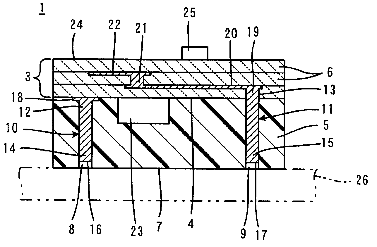
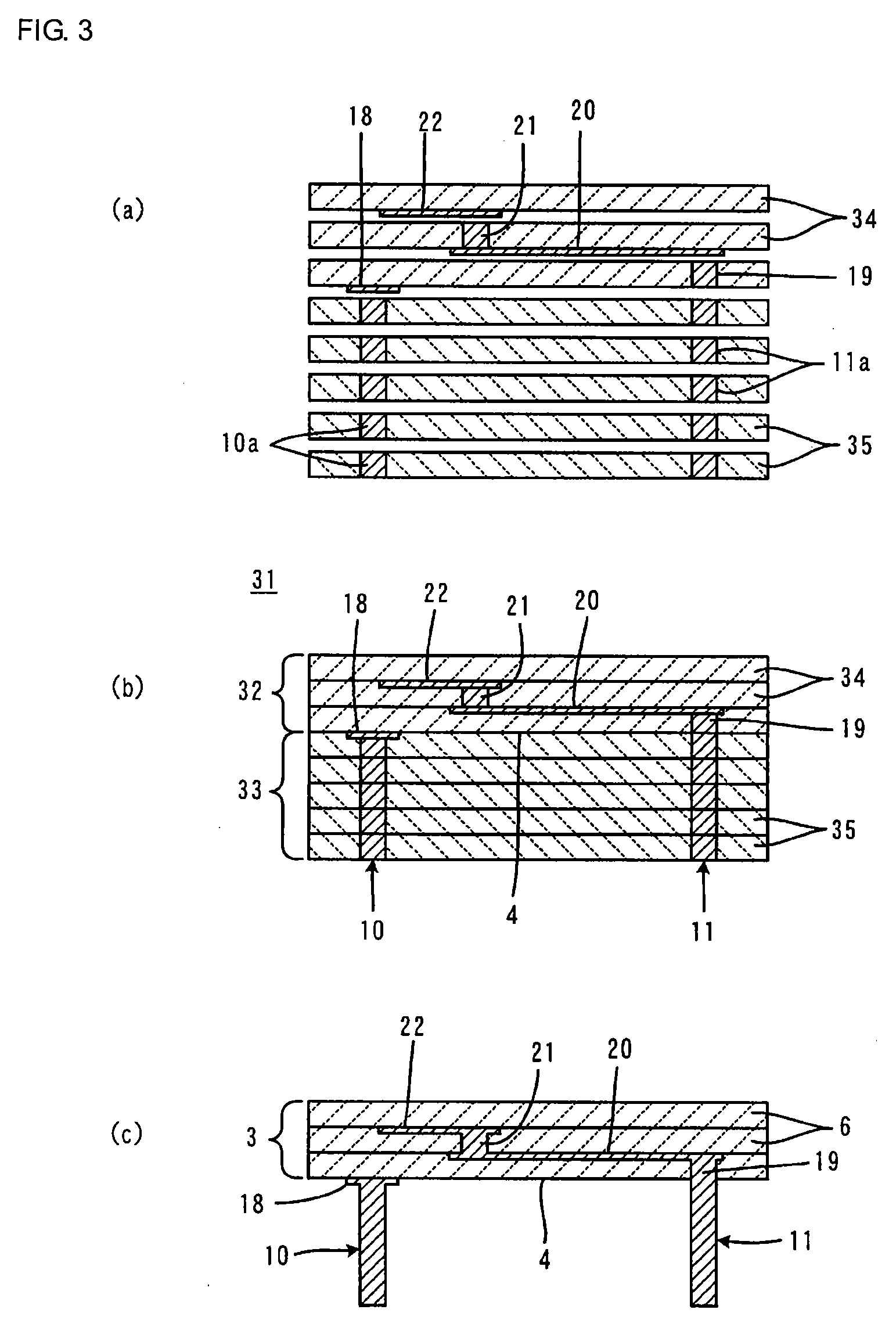
[0076]FIG. 1 to FIG. 3 are views illustrating a first embodiment according to the present invention. In this embodiment, FIG. 1 is a cross-sectional view of a multilayer electronic component 1, FIG. 2 is a partly enlarged cross-sectional view of an electronic device 2 obtained by mounting the multilayer electronic component 1 shown in FIG. 1 on a mounting substrate, and FIG. 3 includes cross-sectional views illustrating a method for manufacturing the multilayer electronic component 1.

[0077] As shown in FIG. 1, the multilayer electronic component 1 has a ceramic substrate 3 and a resin layer 5 formed on a major surface 4 of the ceramic substrate 3. The ceramic substrate 3 has a multilayer structure formed of ceramic layers 6 laminated to each other. The ceramic layer 6 is formed, for example, from a low-temperature firing ceramic material containing Al2O3 as filler and borosilicate glass as a sintering additive. In addition, the resin layer 5 is formed, for example, of an epoxy-base...

Example

[0117]FIG. 9 is a cross-sectional view showing a multilayer electronic component 1e of a sixth embodiment according to the present invention. In FIG. 9, the same reference numerals as in FIG. 1 designate constituent elements corresponding to those shown in FIG. 1, and a duplicate description is omitted.

[0118] In the multilayer electronic component 1e shown in FIG. 9, besides the recess portions 8 and 9, a recess portion 41 is further provided, and an electronic element 42 such as a chip element is received in the recess portion 41. The electronic element 42 is located inside the recess portion 41 further from an opening face thereof.

[0119] In addition, in the resin layer 5, besides the columnar conductors 10 and 11, columnar conductors 43 and 44 are disposed. The columnar conductor 43 reaches the interface between the ceramic substrate 3 and the resin layer 5 and is integrated with a conductor film 45 formed on the major surface 4 of the ceramic substrate 3. In addition, the colum...

Example

[0122]FIG. 10 is a cross-sectional view showing a multilayer electronic component 1f of a seventh embodiment according to the present invention. In FIG. 10, the same reference numerals as in FIG. 1 designate constituent elements corresponding to those shown in FIG. 1, and a duplicate description is omitted.

[0123] In the multilayer electronic component 1f shown in FIG. 10, in particular, the dimension in the height direction of the electronic element 23 on the ceramic substrate 3 is larger than the dimension in the axis line direction of the columnar conductor 10 on the ceramic substrate 3. In addition, the dimensions of the columnar conductors 10 and 11 in the axis line direction are different from each other.

[0124] As is the case of the columnar conductor 10, when the dimension in the axis line direction is decreased, the mechanical strength can be increased for the ceramic substrate 3, and the resistance against a lateral pushing force can also be increased. In addition, when th...


PUM

PropertyMeasurementUnit
Thicknessaaaaaaaaaa
Sizeaaaaaaaaaa
Electrical conductoraaaaaaaaaa

Abstract

A multilayer electronic component having a ceramic substrate and a resin layer mounted on a mounting substrate. Recess portions are formed at an outside-facing major surface side of the resin layer. In the resin layer, columnar conductors are disposed so that axis line directions thereof are aligned in a thickness direction of the resin layer. End portions of the columnar conductors are located inside the recess portions further from opening faces thereof and have end surfaces exposed in the recess portions. When a multilayer electronic component is mounted on a mounting substrate, solder is provided on the end surfaces of the columnar conductors in the recess portions. The thickness of solder used in the above mounting does not interfere with a reduction in size and height of an electronic device that includes the above multilayer electronic component.

Description

CROSS REFERENCE TO RELATED APPLICATIONS [0001] The present application is a continuation of International Application No. PCT / JP2006 / 312300, filed Jun. 20, 2006, which claims priority to Japanese Patent Application No. JP2005-217376, filed Jul. 27, 2005, the entire contents of each of these applications being incorporated herein by reference in their entirety.FIELD OF THE INVENTION [0002] The present invention relates to a multilayer electronic component, an electronic device comprising the multilayer electronic component, and a method for manufacturing a multilayer electronic component, and in particular, relates to a multilayer electronic component having a laminate structure in which a resin layer is formed on a ceramic substrate, an electronic device having the structure in which this multilayer electronic component is mounted on a mounting substrate, and a method for manufacturing a multilayer electronic component. BACKGROUND OF THE INVENTION [0003] As a multilayer electronic c...

Claims


Application Information

Patent Timeline
IPC IPC(8): H01L23/28
CPCH01L21/4853Y10T29/49002H01L23/49816H01L23/49827H01L23/5389H01L24/24H01L24/82H01L2224/24226H01L2924/01002H01L2924/01004H01L2924/01029H01L2924/01033H01L2924/01078H01L2924/01079H01L2924/14H01L2924/1532H01L2924/19041H01L2924/19106H05K1/0306H05K1/111H05K1/183H05K3/245H05K3/28H05K3/284H05K3/3421H05K3/4007H05K3/4611H05K3/4629H05K2201/0367H05K2201/09472H05K2201/096H05K2203/308H01L2924/01005H01L2924/01006H01L2924/01047H01L2924/014H01L21/486H01L2924/15787H01L2924/12042Y02P70/50H01L2924/00
Inventor KIMURA, MASAHIROSAITO, YOSHIFUMI
Owner MURATA MFG CO LTD
Why Eureka
Try Eureka