Structure and method for creating reliable via contacts for interconnect applications

a technology of interconnecting structures and via contacts, applied in the direction of semiconductor devices, semiconductor/solid-state device details, electrical apparatus, etc., can solve the problems of increasing the difficulty of achieving the effect of achieving reliable via to wire connection, no significant impact on resistance or processing complexity, and increasing the reliability and strength of the via to wire connection

Active Publication Date: 2007-11-22
AURIGA INNOVATIONS INC
View PDF19 Cites 40 Cited by
  • Summary
  • Abstract
  • Description
  • Claims
  • Application Information

AI Technical Summary

Benefits of technology

[0010]The present invention provides an interconnect structure and method of fabricating the same which increases the reliability and strength of the via to wire connection, without introducing any damaged regions into the dielectric ma

Problems solved by technology

The major problem encountered in this area today is poor mechanical integrity of deep submicron metal studs embedded in low k dielectric materials, which can cause unsatisfied thermal cycling and stress migration resistance in interconnect structures.
This problem becomes more severe when either new metallization approaches or porous low k dielectric materials are used.
However, the argon sputtering technique that is used to create via gouging in the prior art damages the low k dielectric material.
Because of the requirement of creating the gouging feature, the final interconnect structure includes severe damage that has been introduced into the low k dielectric material from the Ar sputtering process.
The dama

Method used


Image

  • Structure and method for creating reliable via contacts for interconnect applications
  • Structure and method for creating reliable via contacts for interconnect applications
  • Structure and method for creating reliable via contacts for interconnect applications

Examples


Embodiment Construction

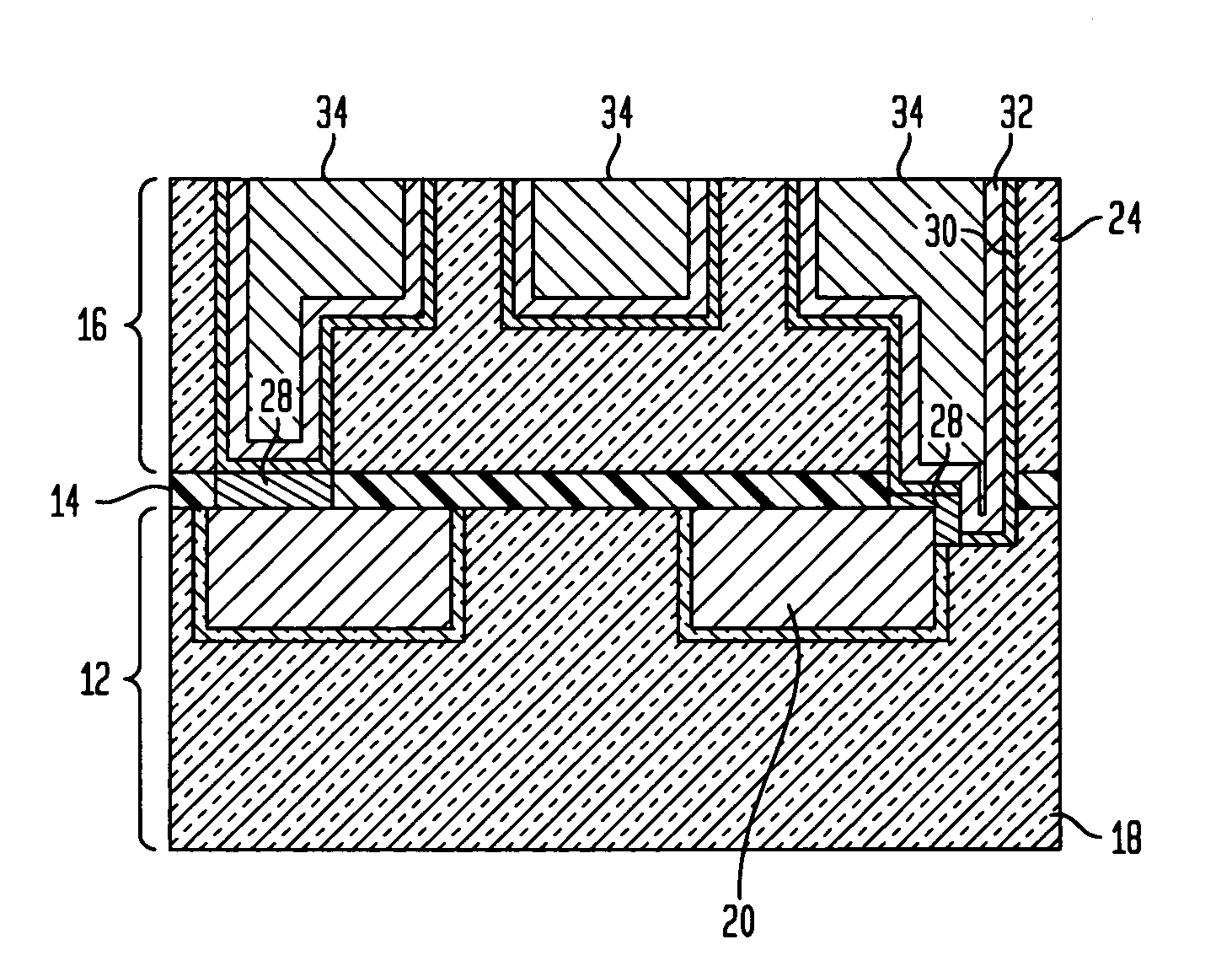
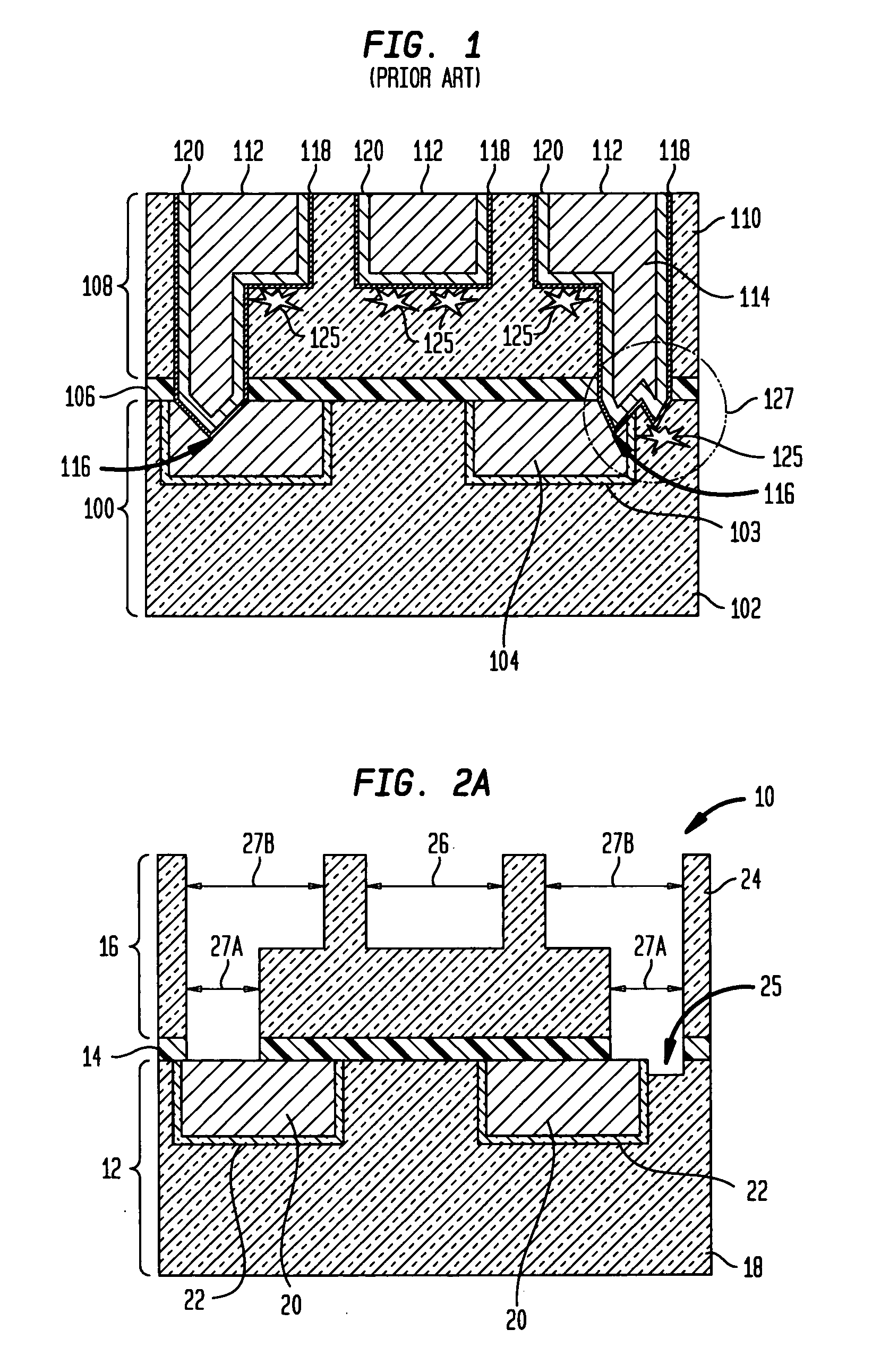
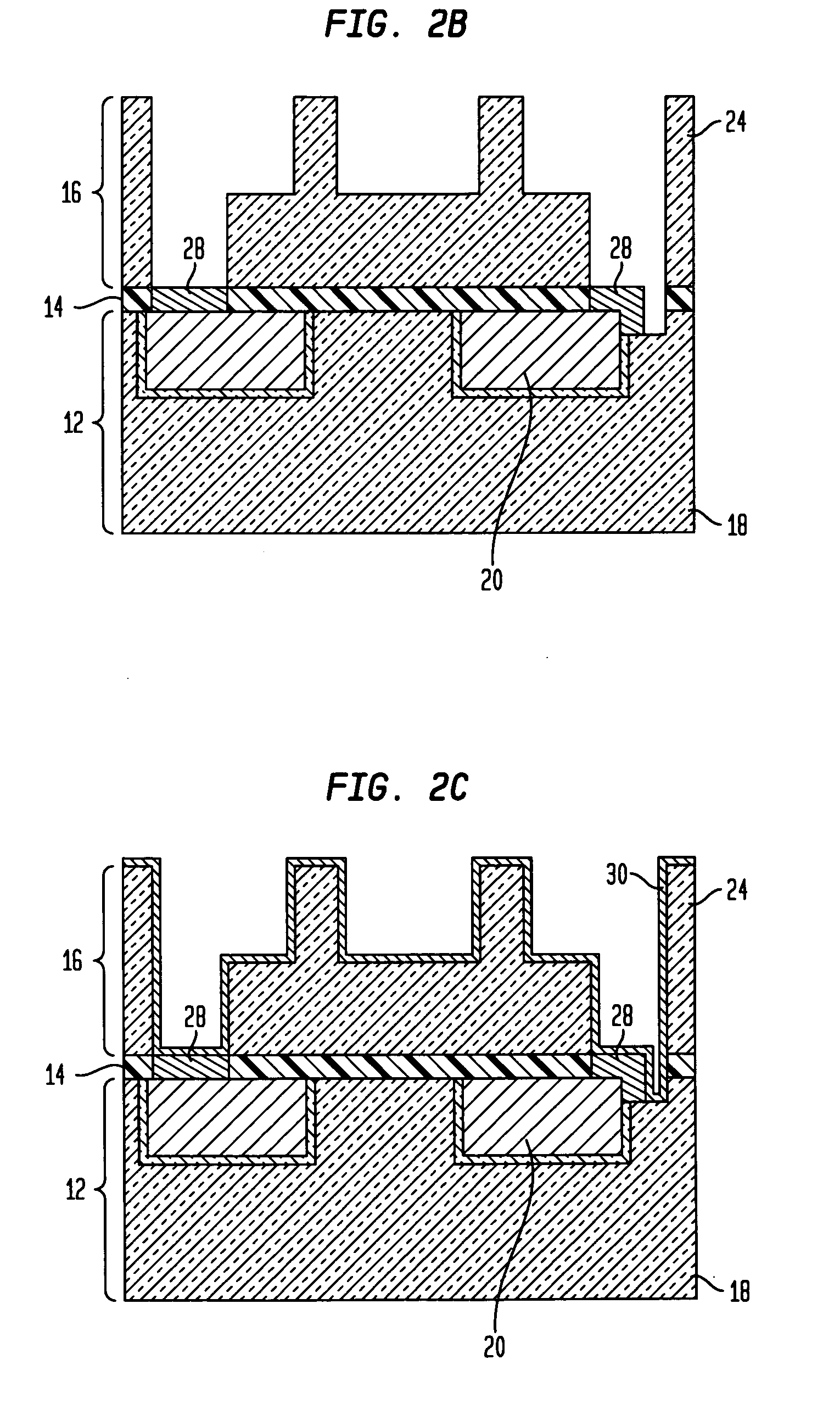
[0037]The present invention, which provides an interconnect structure including a Co-containing alloy located at the interface between the opening of an upper interconnect level and a conductive feature of a lower interconnect level and a method of fabricating the same, will now be described in greater detail by referring to the following discussion and drawings that accompany the present application. The drawings of the present application, which are referred to herein below in greater detail, are provided for illustrative purposes and, as such, they are not drawn to scale.

[0038]In the following description, numerous specific details are set forth, such as particular structures, components, materials, dimensions, processing steps and techniques, in order to provide a thorough understanding of the present invention. However, it will be appreciated by one of ordinary skill in the art that the invention may be practiced without these specific details. In other instances, well-known st...


PUM


Abstract

A reliable and mechanical strong interconnect structure is provided that does not include gouging features in the bottom of the an opening, particularly at a via bottom. Instead, the interconnect structures of the present invention utilize a Co-containing buffer layer that is selectively deposited on exposed surfaces of the conductive features that are located in a lower interconnect level. The selective deposition is performed through at least one opening that is present in a dielectric material of an upper interconnect level. The selective deposition is performed by electroplating or electroless plating. The Co-containing buffer layer comprises Co and at least one of P and B. W may optionally be also present in the Co-containing buffer layer.

Description

FIELD OF THE INVENTION[0001]The present invention relates to a semiconductor structure and a method of fabricating the same. More particularly, the present invention relates to an interconnect structure having increased reliability and strength of the via to wire connection with no significant impact to resistance or processing complexity.BACKGROUND OF THE INVENTION[0002]Generally, semiconductor devices include a plurality of circuits which form an integrated circuit fabricated on a semiconductor substrate. A complex network of signal paths will normally be routed to connect the circuit elements distributed on the surface of the substrate. Efficient routing of these signals across the device requires formation of multilevel or multilayered schemes, such as, for example, single or dual damascene wiring structures. Within a typical interconnect structure, metal vias run perpendicular to the semiconductor substrate and metal lines run parallel to the semiconductor substrate.[0003]As mi...

Claims


Application Information

Patent Timeline
IPC IPC(8): H01L23/52
CPCH01L21/288H01L21/76814H01L21/76816H01L21/76834H01L21/76843H01L2924/0002H01L21/76846H01L21/76852H01L2924/00
Inventor YANG, GHIH-CHAOSTRATEN, OSCAR VAN DER
Owner AURIGA INNOVATIONS INC
Why Eureka
Try Eureka