Image display device

a display device and image technology, applied in the field of image display devices, can solve the problems of difficult to improve the s/n ratio of light sensors, difficult to read high-speed images, and deterioration of the opening area of display pixels, so as to achieve less wrong recognition

Inactive Publication Date: 2007-11-22
HITACHI DISPLAYS
View PDF4 Cites 77 Cited by
  • Summary
  • Abstract
  • Description
  • Claims
  • Application Information

AI Technical Summary

Benefits of technology

[0023]According to the present invention, high-speed reading of a light signal is possible at high S/N ratio, irrespective of luminance of backligh

Problems solved by technology

With the conventional art 1, although it is configured to satisfy the requirements for image inputting and image displaying, the problem that it is difficult to improve S/N ratio of the light sensor still remains.
Enlargement of the light sensor size for higher sensitivity may cause a problem that the sensing area is expanded, resulting in deteriorated rate of opening area of a display pixel.
As a result, S/N ratio of optical signal output that is read out from the light sensor becomes very small, which made high-sensitivity, high-speed reading difficult in the past.
Accordingly, the probl

Method used


Image

  • Image display device
  • Image display device
  • Image display device

Examples


first embodiment

[0051]Hereinafter, concerning a first embodiment of the present invention, the configuration and operations thereof will be described in sequence with reference to FIGS. 1 to 13.

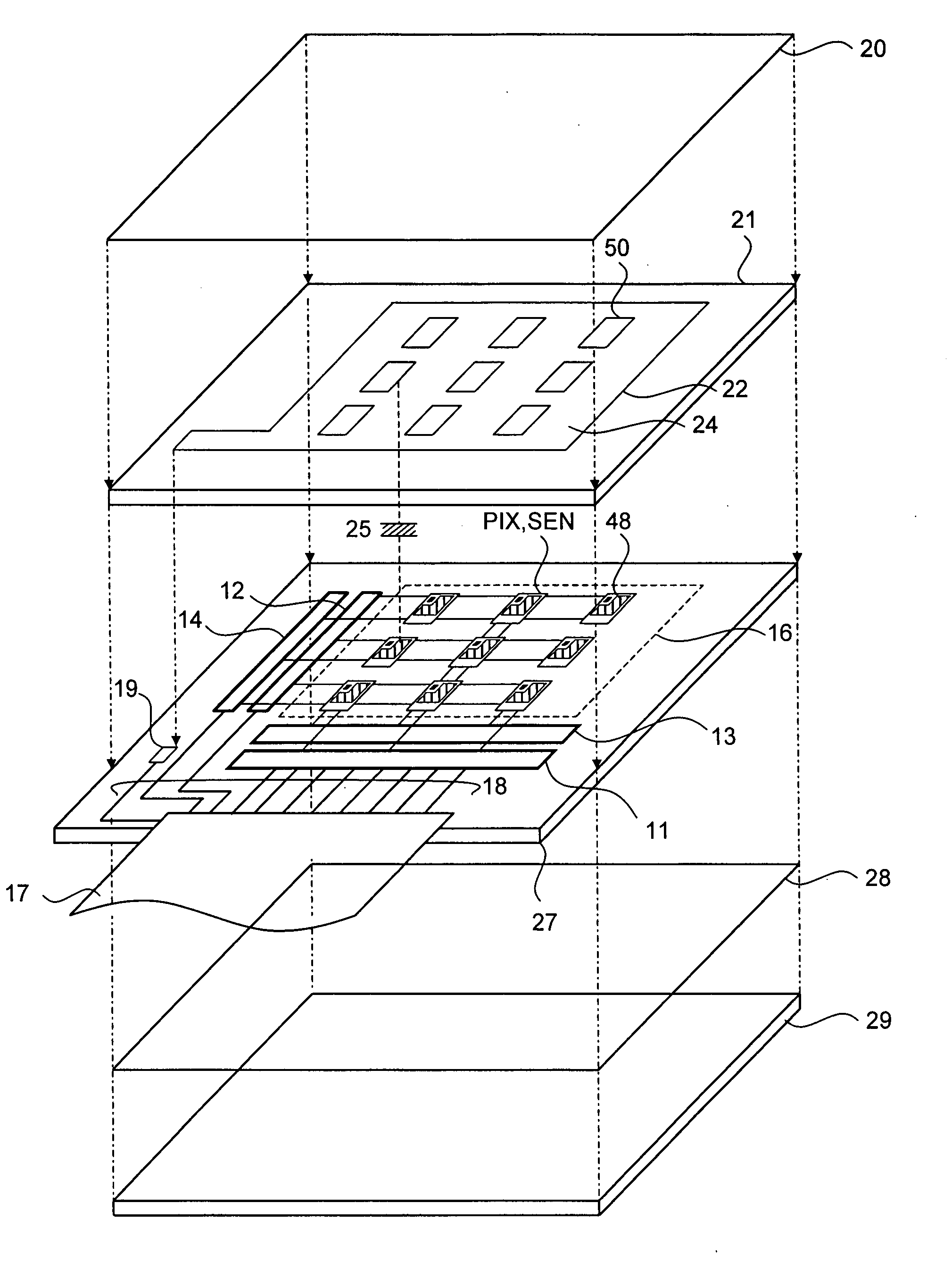
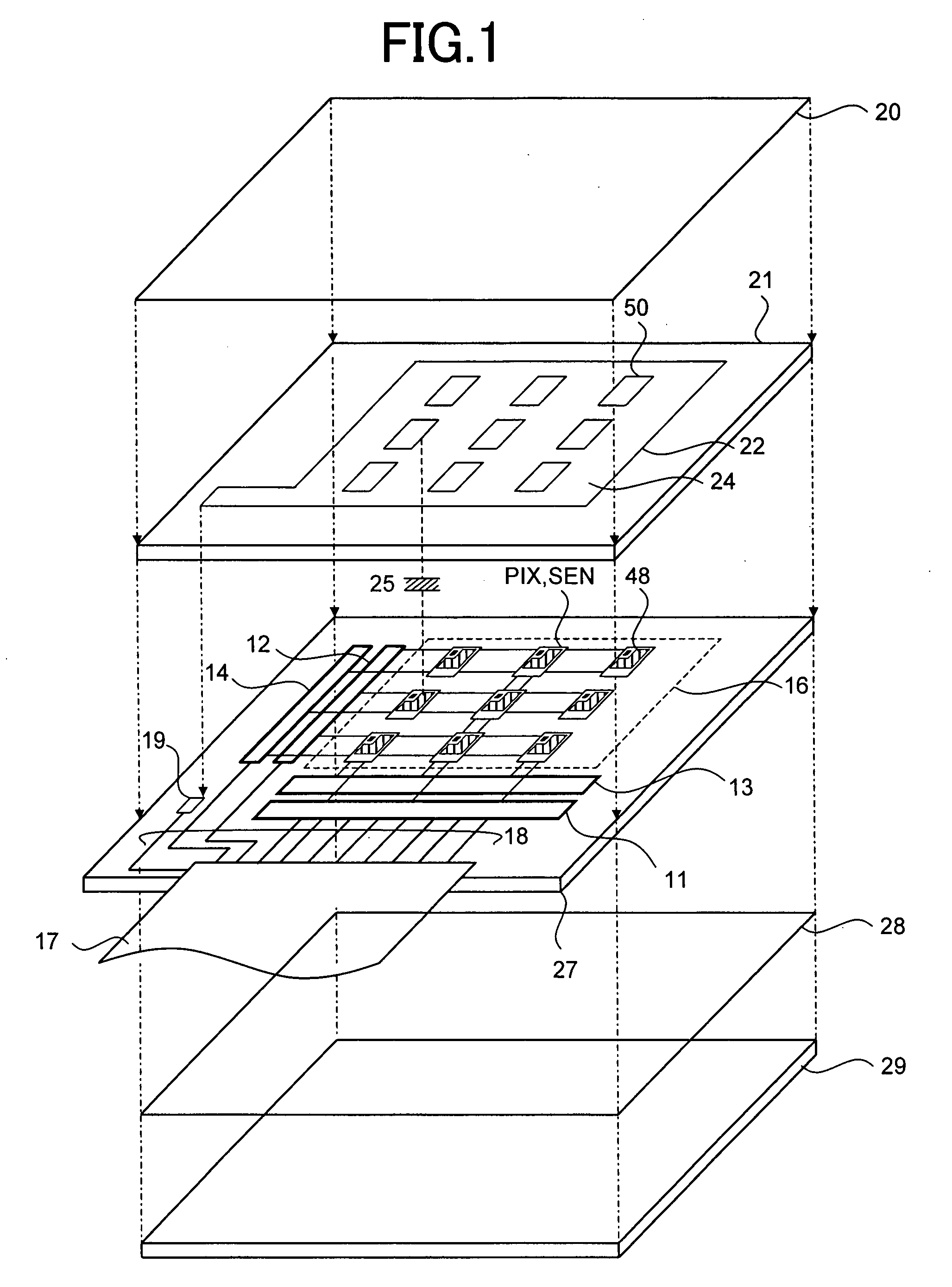
[0052]FIG. 1 shows an exploded perspective view of the structure of an image display device according to the present invention. On the surface of a glass substrate 27, a signal output circuit 11, a gate line scan circuit 12, a sensor circuit 13 and a sensor gate line selection circuit 14 that are formed by using TFTs are arranged. In a display area 16, a display pixel circuit PIX and a photo-sensing circuit SEN, which are manufactured in a TFT manufacturing process, are arranged and formed in a matrix. On the glass substrate 27, a film substrate 17 (FPC: Flexible Printed Circuit) is affixed, and a voltage signal from an external source and voltage that is required for driving the circuit are fed via the film substrate 17.

[0053]Wiring lines 18 which connect the film substrate 17, the signal output circuit 11,...

second embodiment

[0161]Hereinafter, a second embodiment of the image display device according to the present invention will be described in sequence concerning the configuration and operations thereof with reference to FIGS. 14 to 19.

[0162]FIG. 14 shows wavelength dependency of light transmittance of a general color filter that is used in the image display device of the second embodiment. The horizontal axis shows wavelength λ of light and the vertical axis shows light transmittance.

[0163]The light transmittance of a red color filter shows a curve that has its peak at wavelength λR. The light transmittance of a green color filter shows a curve having its peak at wave length λG. The light transmittance of a blue color filter shows a curve having its peak at wavelength λB. In general, the wavelength λB is around 450 nm; λG, around 550 nm; and λR, around 650 nm. The wavelength having highest light transmittance becomes larger in the order of blue, green and red color filters.

[0164]In particular, in the...

third embodiment

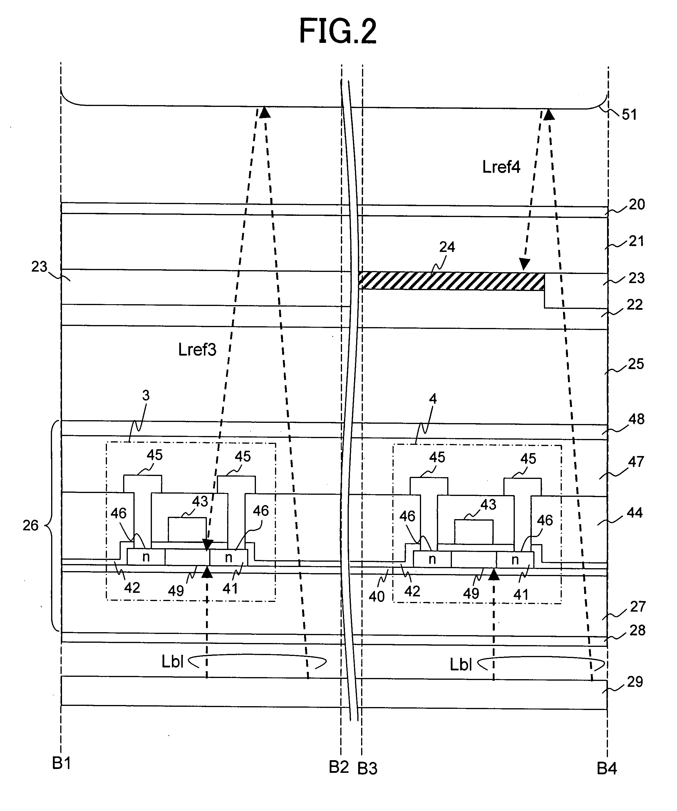
[0217]Hereinafter, a third embodiment of the present invention will be described with reference to FIGS. 22 and 23.

[0218]FIG. 22 shows a layout example of the display pixel circuit PIX and the photo-sensing circuit SEN of the third embodiment. The configuration of the layout example of the display pixel circuit PIX and the photo-sensing circuit SEN of the third embodiment is basically same as that of the first embodiment.

[0219]A different point from the first embodiment is that the metal wiring connected to the drain and the source electrodes on the gate electrode of the photo-sensing TFT 4 is extended by the distance x and the channel layer 49 is extended by the distance y from those in FIG. 12 to form an overlapping area and shield external light, thus preventing external light from being incident on the channel layer 49 of the external photo-sensing TFT 4. Here, the distance x is an overlapping spacing of the gage metal layer 43 and the metal wiring layer 45, the distance y is wi...


PUM


Abstract

The present invention provides an image display device which includes a photo-sensing circuit capable of high-speed light signal reading at high S/N ratio and has a touch-panel function with less influence by disturbance light and less wrong recognition.
The image display device comprises a display unit in which display pixels having thin-film transistors are arranged in a matrix and a plurality of light detection pixels within the display unit. The image display device is configured in such a way that a first light sensing element that receives observation light and a second light sensing element that does not receive observation light are electrically connected, and that a blue color filter and the first light detection pixel are overlapped and a green or a red color filter and the second light detection pixel are overlapped at a light sensing element that outputs potential modulation at the connection point of the first and second light sensing elements.

Description

CLAIM OF PRIORITY[0001]The present application claims priority from Japanese application JP 2006-138689 filed on May 18, 2006, the content of which is hereby incorporated by reference into this application.BACKGROUND OF THE INVENTION[0002]1. Field of the Invention[0003]The present invention relates to an image display device which incorporates an input function that enables inputting of light signal with high S / N ratio.[0004]2. Description of the Related Art[0005]In recent years, image display devices using liquid crystal have been employed popularly as display screens for appliances such as personal computers, mobile phones and PDAs since they have significant advantages of low-profile design, light in weight and low power consumption. Further, the applications are expanded by providing screen input functions such as touch-panel inputting and pen-based inputting, and development of technologies for screen input functions are becoming active. However, incorporation of screen input f...

Claims


Application Information

Patent Timeline
IPC IPC(8): G09G3/00
CPCG02F1/13338G02F1/133512G06F3/042G06F3/0412G06F3/0416G02F2001/13312G02F1/13312
Inventor KINOSHITA, MASAYOSHIKAGEYAMA, HIROSHIAKIMOTO, HAJIME
Owner HITACHI DISPLAYS
Why Eureka
Try Eureka