Power semiconductor module

a technology of power semiconductor modules and semiconductor modules, applied in semiconductor devices, solid-state devices, basic electric elements, etc., can solve the problems that the electromagnetic compatibility of these known power semiconductor modules leaves room for improvement, and achieve the effect of improving electromagnetic compatibility and simple production

Inactive Publication Date: 2007-11-29
SEMIKRON ELECTRONICS GMBH & CO KG
View PDF2 Cites 7 Cited by
  • Summary
  • Abstract
  • Description
  • Claims
  • Application Information

AI Technical Summary

Benefits of technology

[0005]It is an object of the invention to provide a power semiconductor module

Problems solved by technology

These relatively long connections have the drawback that the electromagnetic compatibility of these known power semiconductor modules

Method used


Image

  • Power semiconductor module
  • Power semiconductor module
  • Power semiconductor module

Examples


Embodiment Construction

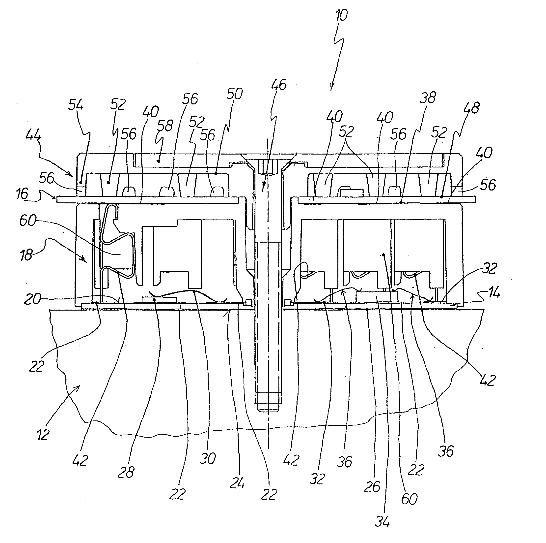
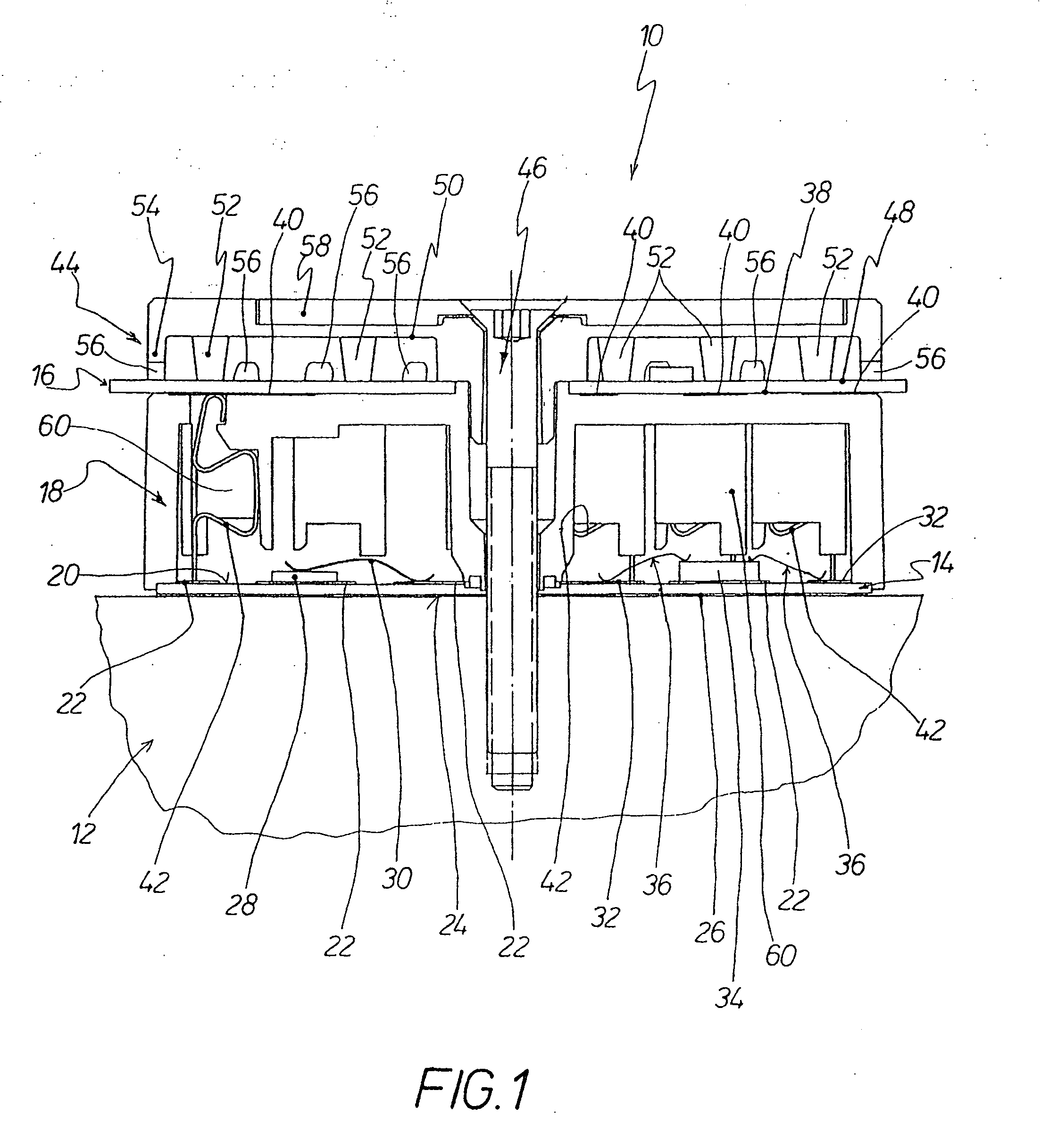
[0015]A power semiconductor module in accordance with the invention is shown in cross-section in FIG. 1, generally at 10. Power semiconductor module 10 is provided for direct assembly on a heat sink 12, drawn in sections. Power semiconductor module 10 has an electrically insulating substrate 14 and a circuit board 16 that is spaced apart from substrate 14 by a housing 18.

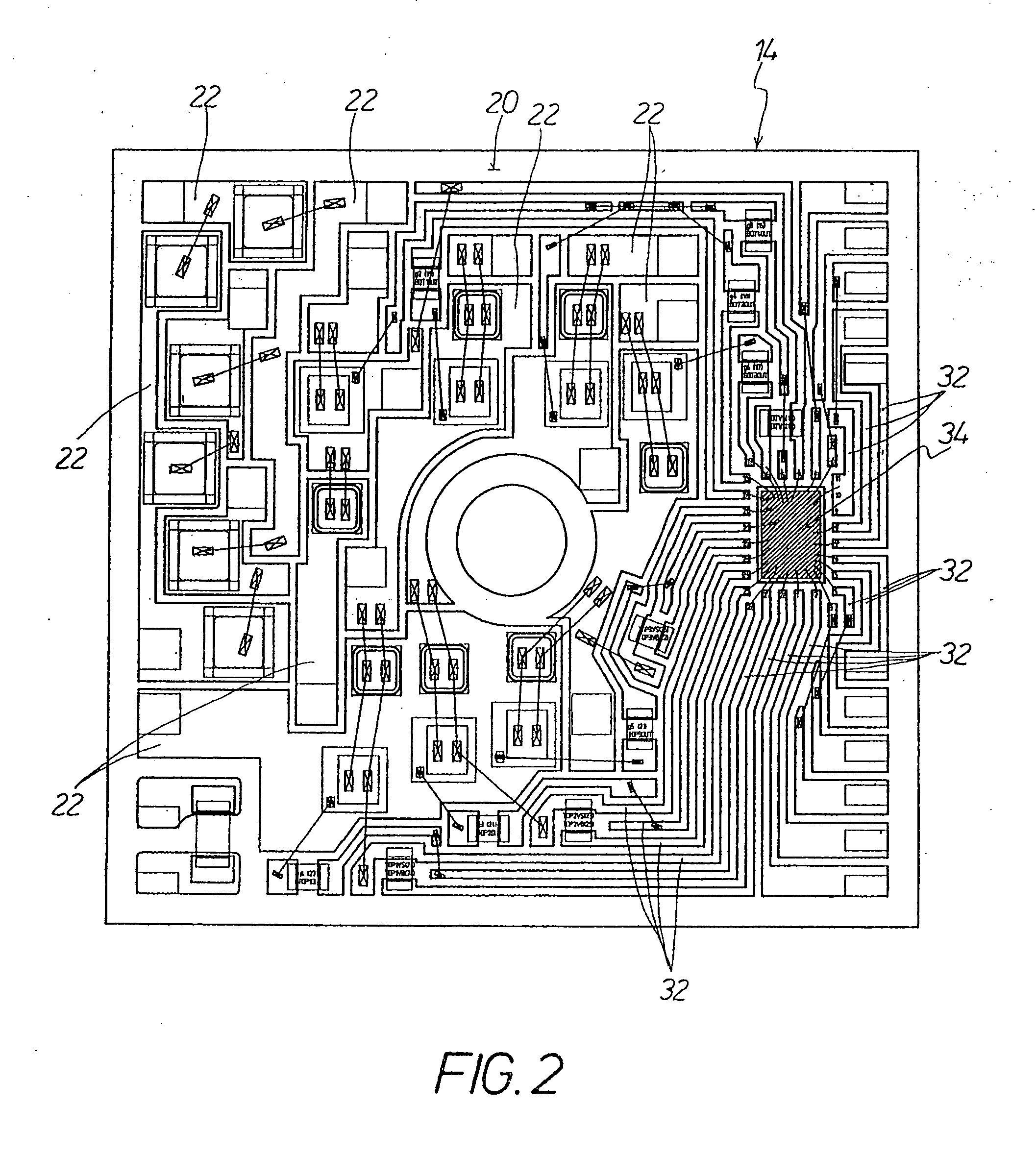
[0016]As can also be seen from FIG. 2, electrically insulating substrate 14 has first conductor tracks 22 disposed on its inside 20 facing the circuit board 16. On the outside 24 of the substrate 14 opposite to inside 20, electrically conductive substrate 14 is provided with a metal layer 26 to thermally couple electrically insulating substrate 14 to heat sink 12.

[0017]Power semiconductor devices 28 are arranged on the inside 20 of substrate 14. Each power semiconductor device 28 is in electrical contact with an associated first conductor track 22 by a bonding wire 30.

[0018]As can be seen clearly, especially from FI...


PUM


Abstract

A power semiconductor module having an electrically insulating substrate, to be arranged with a circuit board. The circuit board is spaced apart from the substrate by a housing. First conductor tracks are disposed inside the substrate, facing the circuit board, for receiving power semiconductor devices which can be driven by a control IC device. Second conductor tracks are provided on the inside of the circuit board facing the substrate. In the housing, elastic connecting elements are pressure-contacted by a rigid pressure body to establish electrical connection between the first and second conductor tracks. An optimum electromagnetic compatibility is achieved due to the fact that IC conductor tracks and the control IC device are also provided on the inside of the substrate.

Description

BACKGROUND OF THE INVENTION[0001]1. Field of the Invention[0002]The invention relates to a power semiconductor module with resilient connecting elements.[0003]2. Description of the Related Art[0004]Such power semiconductor modules are known, for example, from German Patent Nos. DE 103 06 643 B4 and DE 103 16 355 B3, commonly assigned herewith. In these known power semiconductor modules, control IC devices are provided for driving power semiconductor devices on a circuit board provided on the substrate. This circuit board is a so-called custom board, i.e., in these known power semiconductor modules, the control IC devices for the power semiconductor devices provided on the substrate are implemented on the custom board. In such known power semiconductor modules, the substrate and the circuit boards are spaced apart from the substrate by the housing. Long connections are formed between the control IC devices and associated power semiconductor devices. These relatively long connections ...

Claims


Application Information

Patent Timeline
IPC IPC(8): H01L29/76
CPCH01L25/16H05K1/144H01L2224/73265H01L2224/48227H01L2224/32225H01L25/072H01L2224/48472H01L2224/48137H01L2224/48091H01L2924/00012H01L2924/00014H01L2924/00H01L24/73H01L2924/14H01L2224/0603H01L23/02
Inventor POPP, RAINERLEDERER, MARCO
Owner SEMIKRON ELECTRONICS GMBH & CO KG
Why Eureka
Try Eureka