Check patentability & draft patents in minutes with Patsnap Eureka AI!

Semiconductor Memory Device

a memory device and semiconductor technology, applied in the field of semiconductor memory devices, can solve the problems of wasteful consumption of memory space, and achieve the effects of improving data reliability, high rate processing, and improving data reliability

Active Publication Date: 2007-11-29
PANASONIC CORP
View PDF7 Cites 12 Cited by
  • Summary
  • Abstract
  • Description
  • Claims
  • Application Information

AI Technical Summary

Benefits of technology

[0010] The semiconductor memory device of the present invention can improve data reliability since the error detecting / correcting process is provided in copying data in the non-volatile memory between physical blocks. Since the semiconductor memory card, especially according to claim 1 has the error detecting / correcting circuit, after completion of error detecting and correcting of data recorded in a predetermined physical block in the non-volatile memory, data can be transferred and written to a physical block different from the predetermined physical block, therefore data reliability can be improved and high rate processing can be realized since the processing is executed only in the non-volatile memory without transferring data to the memory controller.
[0011] In addition, since the semiconductor memory card according to claim 2 has the error detecting / correcting circuit in the non-volatile memory, data reliability can be improved and high rate processing can be realized since the processing is executed in the non-volatile memory without transferring data to the memory controller when error can be corrected by the error detecting / correcting circuit in the non-volatile memory. Furthermore, when the error cannot be corrected by the error detecting / correcting circuit in the non-volatile memory, data reliability can be further improved since data is written in the non-volatile memory after completion of data transferring to the memory controller and error correcting in the memory controller.
[0012] In addition, since the semiconductor memory card according to claim 3 has only error detecting circuit in the non-volatile memory, copying between blocks can be realized at high rate when error is not detected and price reduction of a non-volatile memory can be realized along with improving reliability.

Problems solved by technology

For this reason, the flash memory has such a problem that memory area is wastefully consumed when written data is overwritten, that is, data is rewritten.

Method used


Image

  • Semiconductor Memory Device
  • Semiconductor Memory Device
  • Semiconductor Memory Device

Examples


embodiment 1

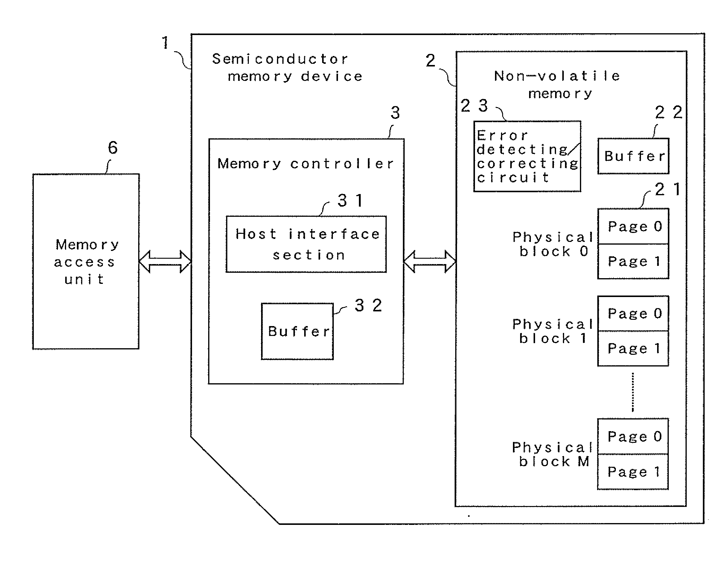
[0030] A configuration of a semiconductor memory device of Embodiment 1 is shown in FIG. 1. A semiconductor memory device 1 mainly includes a non-volatile memory 2 and memory controller 3. The non-volatile memory 2 consists of AND type flash memory. The non-volatile memory 2 includes a plurality of physical blocks 21 (physical block 0˜physical block M) that is a minimum unit of data erasing and that have a size of 4 kB. Each physical block is a minimum unit of data writing and consists of 2 pages (page 0, 1). A size of each page is 2 kB. In Embodiment 1, data is already written in page 0 and page 1 of the physical block 0 and other physical blocks are in an unwritten state, that is, in an erased state.

[0031] In addition, the non-volatile memory 2 includes a buffer 22 for temporarily retaining data at data reading and writing and error detecting / correcting circuit 23 for detecting and correcting error. A specification of the error detecting / correcting circuit 23 is set to have an ab...

embodiment 2

[0040] Next, a semiconductor memory device of Embodiment 2 will be described based on FIG. 4. A basic configuration of the semiconductor memory device in Embodiment 2 is the same as that shown in FIG. 1, but an error detecting / correcting circuit 24 whose error detecting ability is equivalent to and error correcting ability is inferior to those of Embodiment 1 is included in the non-volatile memory 2. In addition, an error correcting circuit 34 having an error correcting ability equivalent to that of Embodiment 1 is included in the memory controller 3. The error correcting circuit 34 may include an error detecting function. These points are different from Embodiment 1.

[0041] An internal processing flow will be described using FIG. 5. Since this flow is almost the same as that shown in FIG. 2, different points will be described. Points different from Embodiment 1 are as follows: when an error is detected in the error detecting / correcting circuit 24 in the non-volatile memory 2 at S11...

embodiment 3

[0042] Next, a semiconductor memory device of Embodiment 3 will be described based on FIG. 6. A basic configuration of the semiconductor memory device in Embodiment 3 is the same as that shown in Embodiment 2, but it is different from Embodiment 2 that only an error detecting circuit 25 is included in the non-volatile memory 2. An internal processing flow is almost the same as that shown in FIG. 2. Points different from Embodiment 2 are as follows: error data detected by the error detecting circuit 25 in the non-volatile memory 2 is all sent to the memory controller 3 via the buffer 22 in the non-volatile memory 2. And, after the data is corrected by the error correcting circuit 34 in the memory controller 3, the corrected data is written to page 1 of the physical block 1 in the non-volatile memory 2 at S113. As described above, the error correcting circuit 34 may include an error detecting function. By using these configurations, since only the error detecting circuit 25 is include...


PUM


Abstract

A semiconductor memory device in which data is not written in a transfer destination under a state including an error when an error occurs at the time of reading data at the transfer destination. The semiconductor memory device (1) comprising a nonvolatile memory (2) having a data writing unit smaller than a physical block is provided with an error detecting / correcting circuit (23) in the non-volatile memory (2). When data stored in a specified block of the non-volatile memory (2) is transferred to a different physical block and written, the error detecting / correcting circuit (23) performs error detection and correction of data.

Description

TECHNICAL FIELD [0001] The present invention relates to a semiconductor memory device that can execute processing such as an error correction when transferring and writing data in a non-volatile memory. BACKGROUND ART [0002] A recording medium for recording digital data such as music contents and image data has various forms such as a magnetic disk, optical disk, and magneto optical disk. A semiconductor memory card, another example of the recording medium, uses non-volatile semiconductor memory such as a flash memory as memory device and is becoming widely used mainly in small-sized portable device such as a digital still camera and cellular phone terminal because the recording medium can be miniaturized. [0003] In the flash memory used as the memory device, an erase unit is different from a writing unit. In addition, the flash memory characteristically cannot overwrite data to a page that is a writing unit in a physical block in which data is already stored. For this reason, the f...

Claims


Application Information

Patent Timeline
Patent Type & Authority Applications(United States)
IPC IPC(8): G06F12/16G11C16/06G11C29/00G11C16/22G11C16/34
CPCG06F11/1068G11C2029/0409G11C16/3418G11C16/22G11C16/34G11C29/00G11C16/16
Inventor TAMURA, KAZUAKIIZUMI, TOMOAKIKASAHARA, TETSUSHINAKANISHI, MASAHIROMATSUNO, KIMINORIINOUE, MANABU
Owner PANASONIC CORP
Features
  • R&D
  • Intellectual Property
  • Life Sciences
  • Materials
  • Tech Scout
  • Unparalleled Data Quality
  • Higher Quality Content
  • 60% Fewer Hallucinations
Learn More