
Melt surface position monitoring apparatus in silicon single crystal growth process

a single crystal growth and melt surface technology, applied in the direction of crystal growth process, polycrystalline material growth, crystal growth process, etc., can solve the problems of difficult to control the melt surface level in a stereotyped manner, complicated monitoring of the melt surface position, etc., and achieve high precision

Active Publication Date: 2007-12-06
SUMCO CORP
View PDF18 Cites 3 Cited by
  • Summary
  • Abstract
  • Description
  • Claims
  • Application Information

AI Technical Summary

Benefits of technology

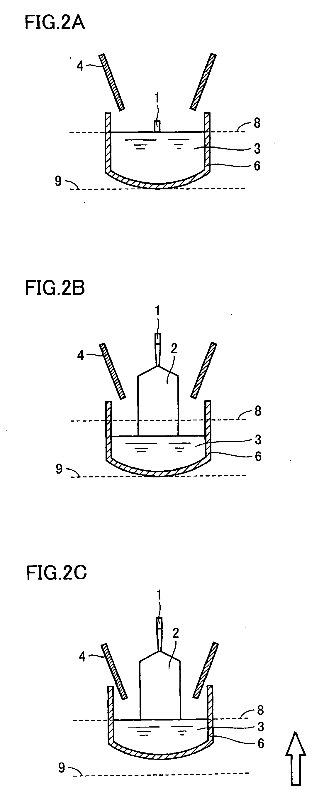
[0025]The present invention, which has been made in view of the problems discussed above, has its object to provide a melt surface position monitoring apparatus making it possible to cope with every change in melt surface position in the process of silicon single crystal growth so as to prevent in advance the melt from coming into contact with the thermal shield and / or water-cooling structure, among others.
[0055]When the estimated melt surface position passes the upper limit set in advance and approaches the thermal shield, an alarm goes off and, further, when the melt surface comes into contact with the thermal shield or approaches the water-cooling structure, an alarm goes off when in need and, at the same time, the crucible is forcedly stopped from moving and thereby a serious accident such as a steam-induced explosion due to the melt coming into contact with the coolant water can be prevented.

Problems solved by technology

In case of remelting during the process of silicon single crystal growth, the monitoring of the melt surface position becomes very complicated, as mentioned above, and, therefore, it is difficult to control the melt surface level in a stereotyped manner.

Method used


Image

  • Melt surface position monitoring apparatus in silicon single crystal growth process
  • Melt surface position monitoring apparatus in silicon single crystal growth process
  • Melt surface position monitoring apparatus in silicon single crystal growth process

Examples


examples

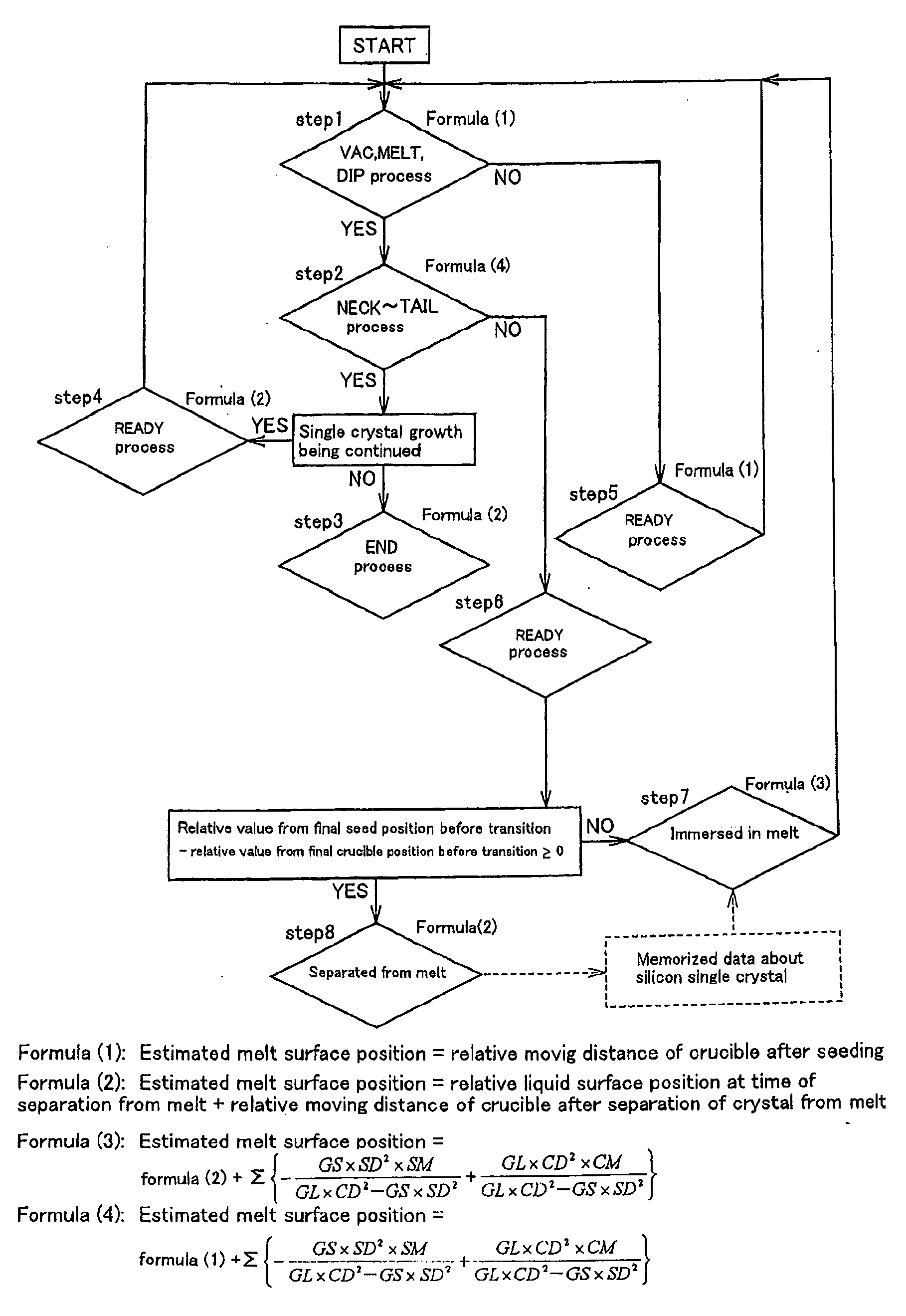
[0090]Referring to a flow chart, the operations of the melt surface position monitoring apparatus of the present invention for use in the silicon single crystal growth process utilizing the CZ method are described.

[0091]FIG. 9 is a flow chart illustrating the operations of the melt surface position monitoring apparatus of the present invention in the silicon single crystal growth process. In the branching in each process shown in FIG. 9, that the operation in question is smoothly carried out is designated by YES and that crystal defects such as dislocation is detected, is designated by NO.

[0092]In the description that follows, “END process” means a process comprising monitoring the liquid surface position for 2 hours following turning off the power supply to the heater for melting silicon and then finishing the liquid surface position monitoring operation. “READY process” has the same meaning as the transition process mentioned above and means a process comprising selecting the form...


PUM


Abstract

The liquid surface position of the melt in the crucible in the silicon single crystal growth process utilizing the Czochralski method is monitored using the melt surface position on the occasion of seeding as a reference position and an estimated melt surface position can be calculated according to every situation, so that the distance between the melt and the thermal shield or water-cooling structure can be controlled with high precision. When the estimated melt surface position passes a preset upper limit and approaches the thermal shield, an alarm goes off and, further, when the melt comes into contact with the thermal shield or approaches the water-cooling structure, an alarm goes off if desired and, at the same time, the crucible is forcedly stopped from moving, so that a serious accident such as steam-incurred explosion resulting from the melt coming into contact with the water-cooling structure can be prevented. Accordingly, the apparatus can be widely applied as a melt surface position monitoring apparatus making it possible to safely operate any silicon single crystal growth apparatus utilizing the Czochralski method.

Description

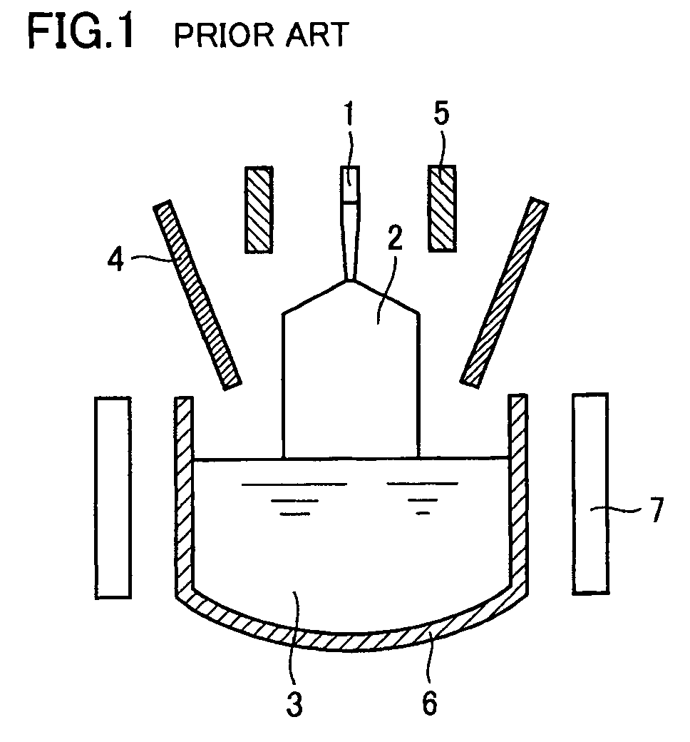
FIELD OF THE INVENTION[0001]The present invention relates to an apparatus for monitoring the melt surface position in a silicon single crystal growth process employing the Czochralski method and, more particularly to a melt surface position monitoring apparatus which makes it possible to cope with every change in liquid surface position during a period from melting raw materials for the crystal to solidification of the melt after completion of the process to prevent every predictable emergency, for example the contact of the melt with a thermal shield and a water-cooling structure or the like.DESCRIPTION OF THE RELATED ART[0002]Silicon single crystals currently used in manufacturing substrates for forming circuit elements such as large scale integrated circuits (LSI) are mostly pulled up by the Czochralski method (hereinafter referred to as “CZ method” for short).[0003]In growing silicon single crystals by the CZ method, raw materials of lumpy polycrystalline silicon charged into a ...

Claims


Application Information

Patent Timeline
IPC IPC(8): C30B15/00C30B27/02C30B23/00
CPCC30B15/20Y10T117/1004Y10T117/1012Y10T117/10Y10T117/1072Y10T117/1032Y10T117/1024Y10T117/1008C30B29/06
Inventor HAYAKAWA, HIROSHIMAEDA, TOKUJI
Owner SUMCO CORP
Learn More