Digital Voltage Level Shifter

a voltage level shifter and digital technology, applied in the field of digital voltage level shifters, can solve the problems of consuming power and affecting the operation of the circuit, and achieve the effect of reducing increasing the difficulty of the problem

Inactive Publication Date: 2007-12-06
INFINEON TECH AG
View PDF15 Cites 15 Cited by
  • Summary
  • Abstract
  • Description
  • Claims
  • Application Information

AI Technical Summary

Benefits of technology

[0004] In general, the present invention relates to a digital voltage level shifter for converting an input signal with a low voltage swing to an output signal with a high voltage swing comprising one or more protection transi

Problems solved by technology

The problem becomes more difficult as CMOS technology moves to lower supply voltages for the main logic of the chip, together with smaller geometries.
Existi

Method used


Image

  • Digital Voltage Level Shifter
  • Digital Voltage Level Shifter
  • Digital Voltage Level Shifter

Examples


Embodiment Construction

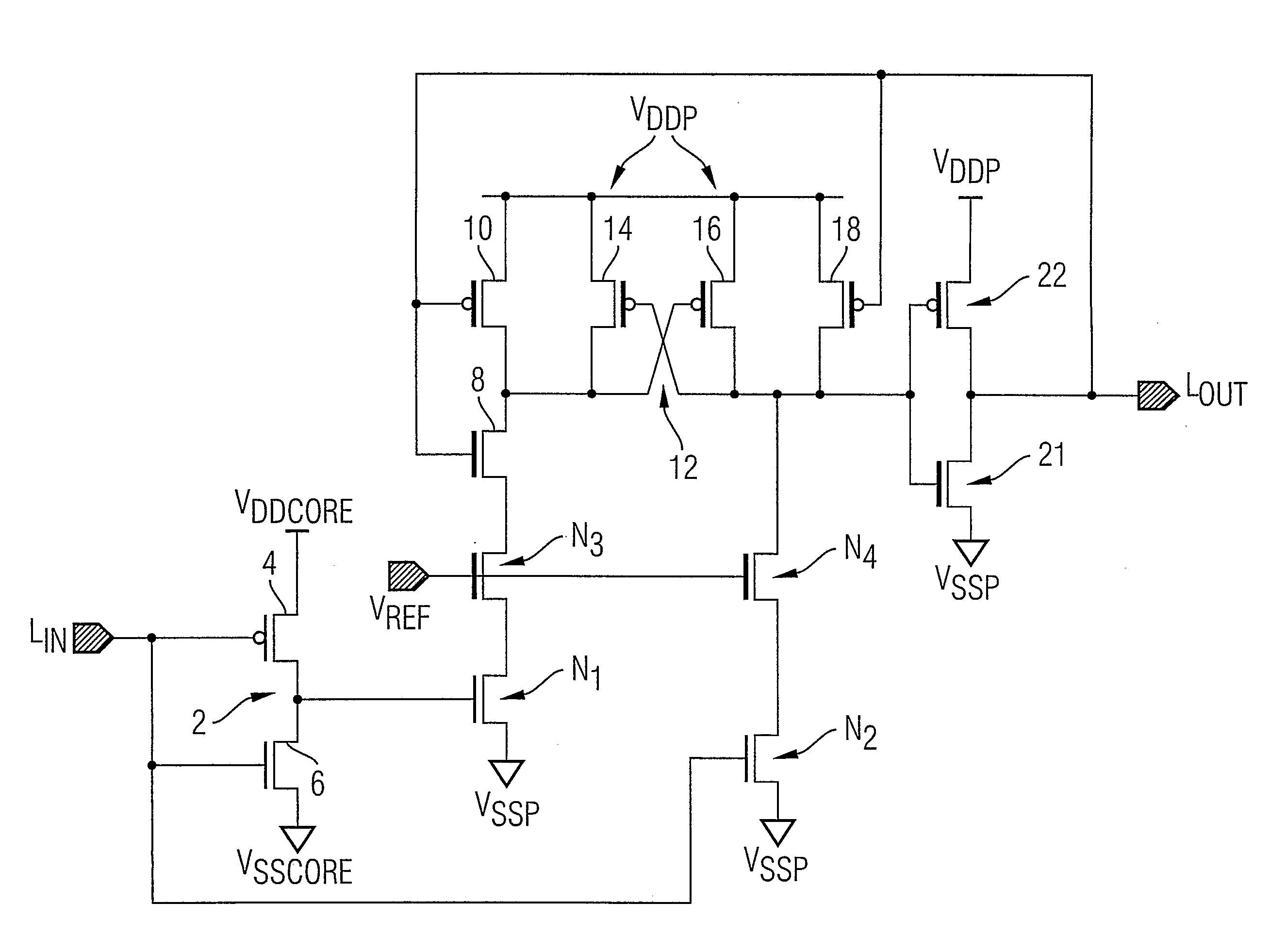
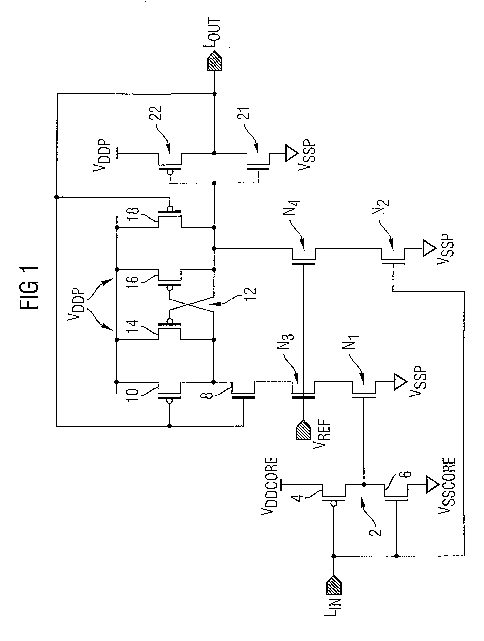
[0016]FIG. 1 shows a circuit diagram of a conventional system for shifting voltage signal levels to a higher range (domain). The system comprises an inverter stage 2 comprising two CMOS transistors 4, 6. The output of the inverter stage 2 is coupled to the gate of a thin gate NMOS transistor N1. The input signal LIN is also coupled to the gate of a further thin gate NMOS transistor N2. The sources of transistors N1 and N2 are coupled to ground (VSSP) and the drains of transistors N1 and N2 are coupled to the sources of two further NMOS transistors N3 and N4 respectively. The gates of transistors N3 and N4 are connected to a reference voltage VREF.

[0017] The drain of N3 is connected to the source of a further transistor 8 which, together with another transistor 10, forms a second inverting stage, the output of which is coupled to a bistable circuit 12 formed by two cross-coupled transistors 14, 16. The drain of N4 is coupled to the other input to the bistable stage 12, to the drain ...


PUM


Abstract

A digital voltage level shifter for converting an input signal with a low voltage swing to an output signal with a high voltage swing comprises a first inverter stage for generating an inverted signal from an input signal, the inverted signal having a voltage swing between a core voltage and ground, and a second inverter stage for producing an anti-phase signal from the inverted input signal, the anti-phase signal having a voltage swing between the core voltage and ground. The first and second inverters each drive a respective thin gate NMOS transistor connected in cascode with a respective NMOS transistor. The sources of the first and second thin gate NMOS transistors are connected to ground. The gates of the NMOS transistors are connected to the output of the respective inverters through a respective capacitor and are referenced to the core voltage through a respective resistor. The drains of the NMOS transistors are connected to an output circuit to provide an output signal having a voltage higher than the core voltage.

Description

FIELD OF THE INVENTION [0001] The present invention relates to a digital voltage level shifter for converting an input signal with a low voltage swing to an output signal with a high voltage swing. BACKGROUND OF THE INVENTION [0002] In VLSI integrated circuits, particularly in the more complex circuits such as microprocessors or digital signal processors, it is often necessary to transfer signals from one voltage domain (range) to another. This may be required to be achieved at high speed and without damage to the transistors involved. The problem becomes more difficult as CMOS technology moves to lower supply voltages for the main logic of the chip, together with smaller geometries. Existing solutions generally require reference voltage supplies which must be either supplied externally or generated within the chip and therefore consume power. [0003] In view of the foregoing problems requirements, a need exists for a method and / or system for which does not suffer from the above disa...

Claims


Application Information

Patent Timeline
IPC IPC(8): H03K3/356
CPCH03K17/102H03K3/356147
Inventor GOEL, MAYANKAGARWAL, PRABHAT
Owner INFINEON TECH AG
Why Eureka
Try Eureka