Photoelectric-conversion-layer-stack-type color solid-state imaging device

Active Publication Date: 2007-12-06
FUJIFILM CORP
View PDF4 Cites 33 Cited by
  • Summary
  • Abstract
  • Description
  • Claims
  • Application Information

AI Technical Summary

Benefits of technology

[0020]According to the invention, the color separation performance is improved by the color filter layers and the efficiency of light utilization is increased because no color filter layers are formed over the first photodiodes. Where the colo

Problems solved by technology

Although the color separation performance is improved, the above-described hybrid imaging device is still insufficient to take high-quality color im

Method used


Image

  • Photoelectric-conversion-layer-stack-type color solid-state imaging device
  • Photoelectric-conversion-layer-stack-type color solid-state imaging device
  • Photoelectric-conversion-layer-stack-type color solid-state imaging device

Examples


embodiment 1

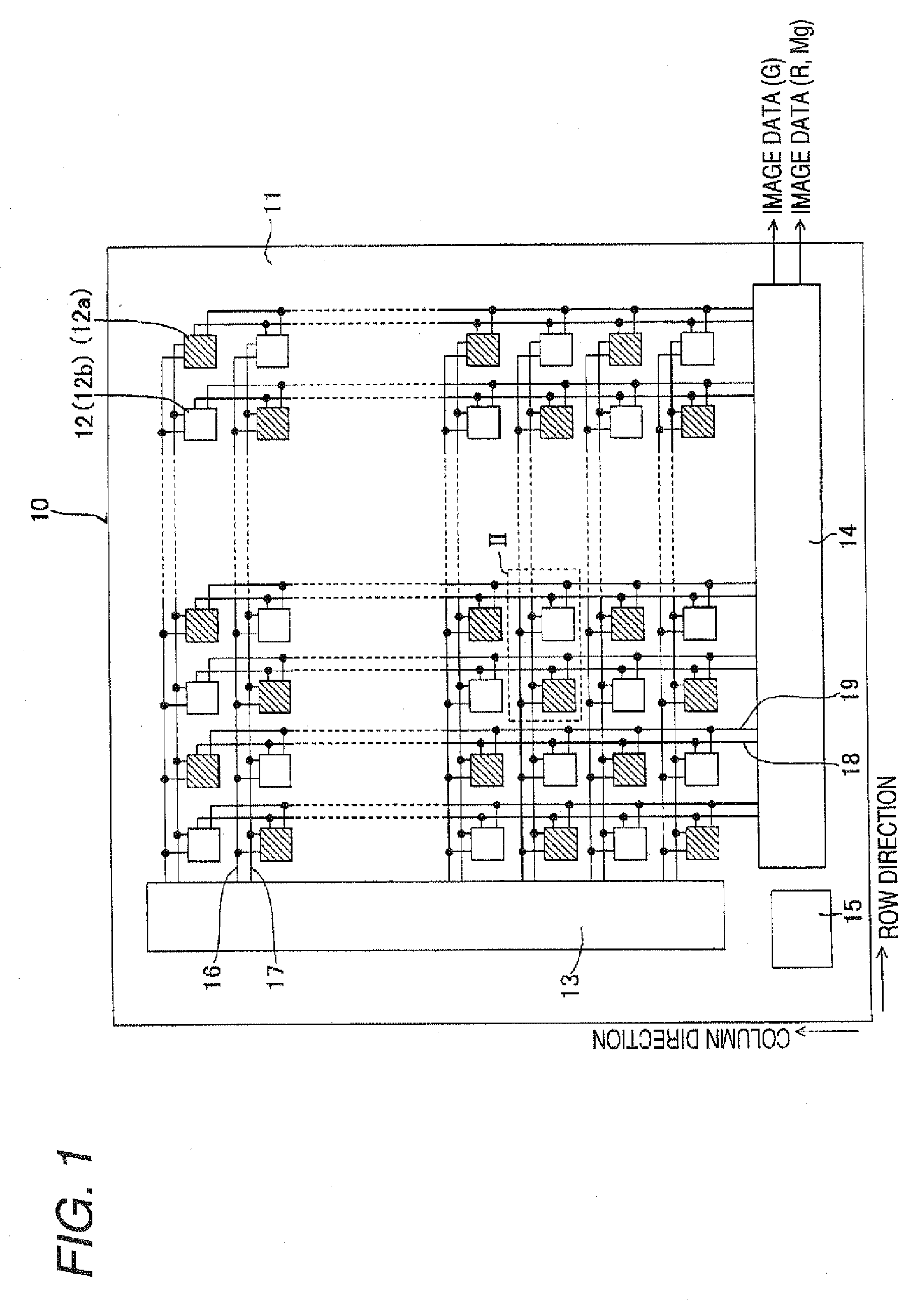
[0043]FIG. 1 schematically shows the surface of a photoelectric-conversion-layer-stack-type color solid-state imaging device according to the embodiment of the invention. In the photoelectric-conversion-layer-stack-type color solid-state imaging device 10 according to the embodiment, plural pixels 12 are arranged in square Lattice form on a photodetecting surface of a substrate 11.

[0044]The pixels 12 are classified into two kinds of pixels 12a and 12b. The pixels 12a and the pixels 12b are formed on the photodetecting surface in checkered form. Alternatively, rows (or columns) of pixels 12a arranged in stripes and rows (or columns) of pixels 12b arranged in stripes are arranged alternately.

[0045]A row-selection scanning section 13 is provided adjacent to the left sideline of the substrate 11 and an image signal processing section 14 is provided adjacent to the bottom sideline. A control section 15 for generating timing pulses and control signals is provided at a proper position.

[004...

embodiment 2

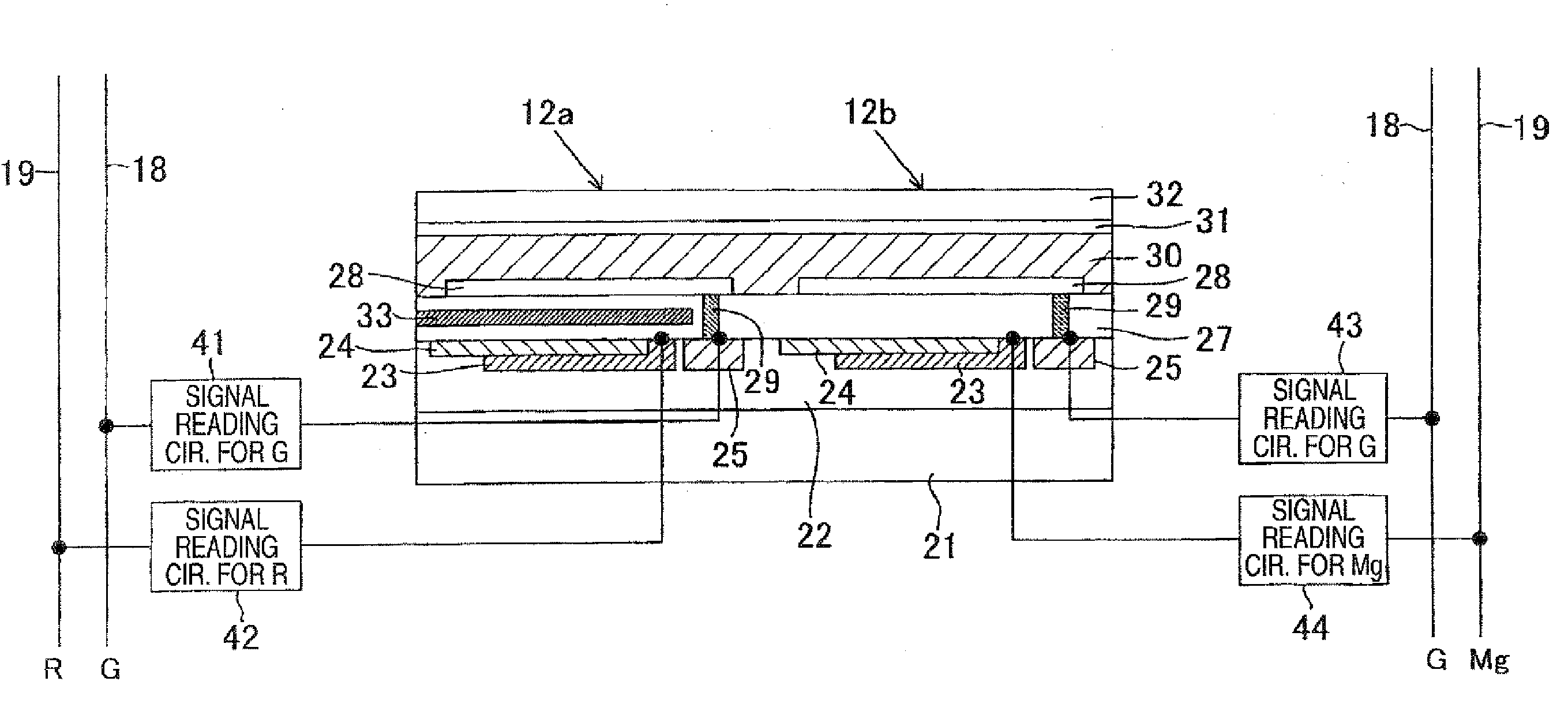
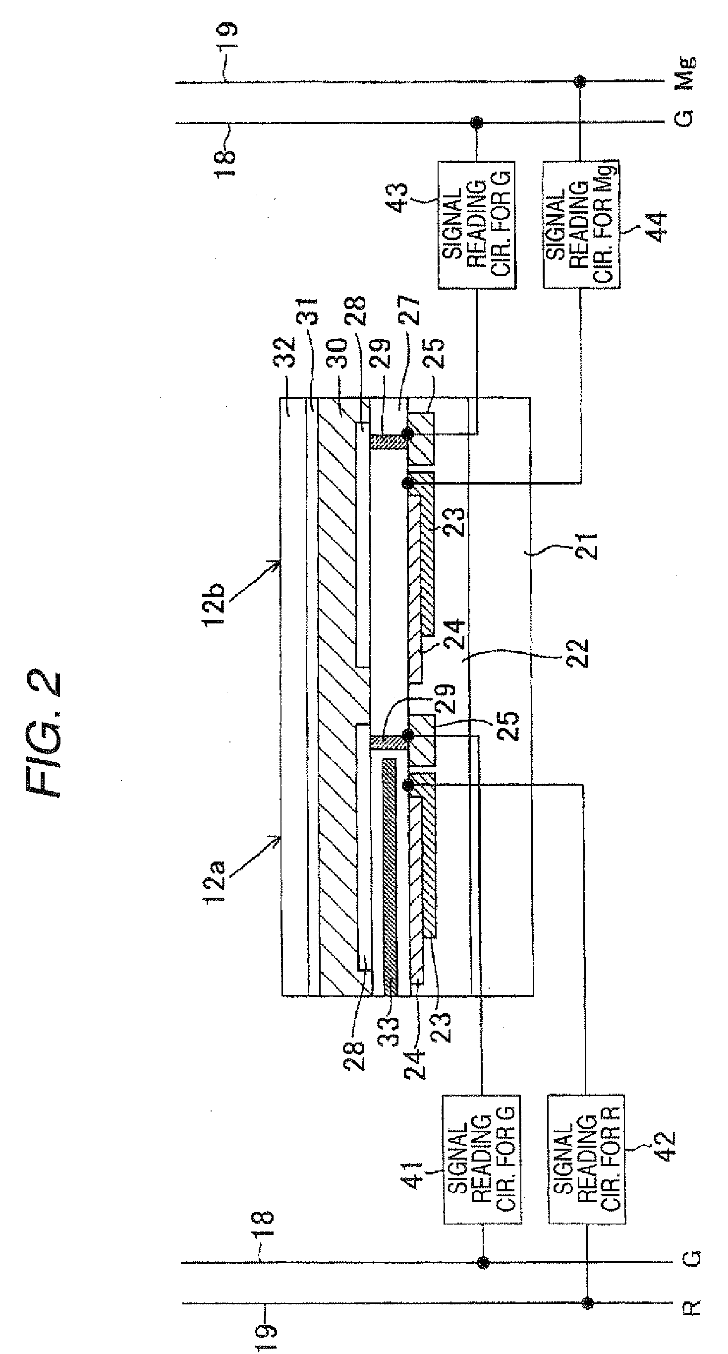
[0074]FIG. 4 is a schematic sectional view of a hybrid photoelectric-conversion-layer-stack-type color solid-state imaging device according to a second embodiment of the invention. The photoelectric-conversion-layer-stack-type color solid-state imaging device according to this embodiment has approximately the same configuration as that according to the first embodiment shown in FIG. 2 and is different from the latter only in that the color filter layers are made of an organic material. Therefore, the same layers etc. as shown in FIG. 2 are given the same symbols as the corresponding ones in FIG. 2 and will not be described below. Only different layers etc. will be described.

[0075]In the photoelectric-conversion-layer-stack-type color solid-state imaging device according to this embodiment, a smooth layer 51 made of an organic material is formed between the transparent insulating layer 27 and the pixel electrode layer 28. In each pixel 12a, a color filter layer 52 for transmission of...


PUM


Abstract

A color solid-state imaging device including: a semiconductor substrate; a photoelectric conversion layer provided over the semiconductor substrate, for absorbing light of a first color among three primary colors so as to generate photocharges; plural charge storage regions arranged in a surface layer of the semiconductor substrate, for storing the photocharges; plural first photodiodes arranged in the surface layer of the substrate, for detecting mixed light of second and third colors among the three primary colors that has passed through the photoelectric conversion layer and for storing generated photocharges; plural second photodiodes arranged in the surface layer of the semiconductor substrate, for detecting light of the second color of the mixed light that has passed through the photoelectric conversion layer and for storing generated photocharges; color filter layers provided over the second photodiodes, for interrupting light of the third color; and signal reading units as defined herein.

Description

FIELD OF THE INVENTION[0001]The present invention relates to a photoelectric-conversion-layer-stack-type color solid-state imaging device in which incident light of one of the three primary colors is detected by a photoelectric conversion layer laid on a semiconductor substrate and incident light of the other two colors that has passed through the photoelectric conversion layer is detected by photoelectric conversion elements (photodiodes) formed in the semiconductor substrate. In particular, the invention relates to a photoelectric-conversion-layer-stack-type color solid-state imaging device which is high in color separation performance and efficiency of light utilization.BACKGROUND OF THE INVENTION[0002]In single-plate color solid-state imaging devices as typified by CCD image sensors and CMOS image sensors, three or four kinds of color filters are arranged in mosaic form on an arrangement of photoelectric conversion pixels. With this structure, color signals corresponding to the ...

Claims


Application Information

Patent Timeline
IPC IPC(8): H04N9/04H01L27/14H01L27/146H01L31/08H04N5/335H04N5/369
CPCH01L27/14609H01L27/14621H01L27/14647H04N2209/047H04N9/045H04N2209/045H01L27/307H01L27/14627H10K39/32H01L27/146
Inventor GOTO, TAKASHISUZUKI, NOBUO
Owner FUJIFILM CORP
Why Eureka
Try Eureka