Electro-optical device, method for manufacturing electro-optical device, and electronic apparatus

a manufacturing method and electrooptical technology, applied in the field of electrooptical devices, can solve the problems of reduced manufacturing efficiency, disadvantageous cost of color liquid crystal display, and inability to individually adjust the reflective section and the transmissive section to a desired color, so as to increase the number of manufacturing steps, reduce the cost of manufacturing, and improve the effect of manufacturing efficiency

Inactive Publication Date: 2007-12-06
JAPAN DISPLAY WEST
View PDF6 Cites 0 Cited by
  • Summary
  • Abstract
  • Description
  • Claims
  • Application Information

AI Technical Summary

Benefits of technology

[0022]The subpixel regions can be formed so as to have a color hue different from the color hues of color resists of primary colors without using an additional color resist in such a manner that the arrangement of the color layers having different color hues in at least one of the subpixel regions is adjusted. Therefore, the color hue of the subpixel region having the color layers can be adjusted without causing an increase in manufacturing cost or an increase in the number of manufacturing steps. That is, the electro-optical device can be efficiently manufactured so as to display an image with high color reproducibility.
[0023]Furthermore, the present invention provides an electronic apparatus including any one of the above electro-optical devices. In the electro-optical devices, the color hues of the subpixel regions are adjusted without causing an increase in manufacturing cost or an increase in the number of manufacturing steps. The electronic apparatus can be efficiently manufactured so as to display an image with high color reproducibility.

Problems solved by technology

Therefore, the color liquid crystal display is disadvantageous in cost.
This leads to a reduction in manufacturing efficiency.
In the color liquid crystal display, the color of each subpixel region cannot be varied although the reflective section and the transmissive section can be varied in color density; hence, the reflective section and the transmissive section cannot be individually adjusted to a desired color.

Method used


Image

  • Electro-optical device, method for manufacturing electro-optical device, and electronic apparatus
  • Electro-optical device, method for manufacturing electro-optical device, and electronic apparatus
  • Electro-optical device, method for manufacturing electro-optical device, and electronic apparatus

Examples


first embodiment

[0049]A first embodiment provides an Electro-optical device, which may be a liquid crystal display that includes a plurality of subpixel regions for forming a display field and also includes a color filter including a plurality of color layers of which at least one is of an additive primary color.

[0050]The liquid crystal display is characterized in that the color filter includes the color layers having different color hues and at least two of the color layers are arranged in at least one of subpixel regions so as not to overlap with each other in plan view.

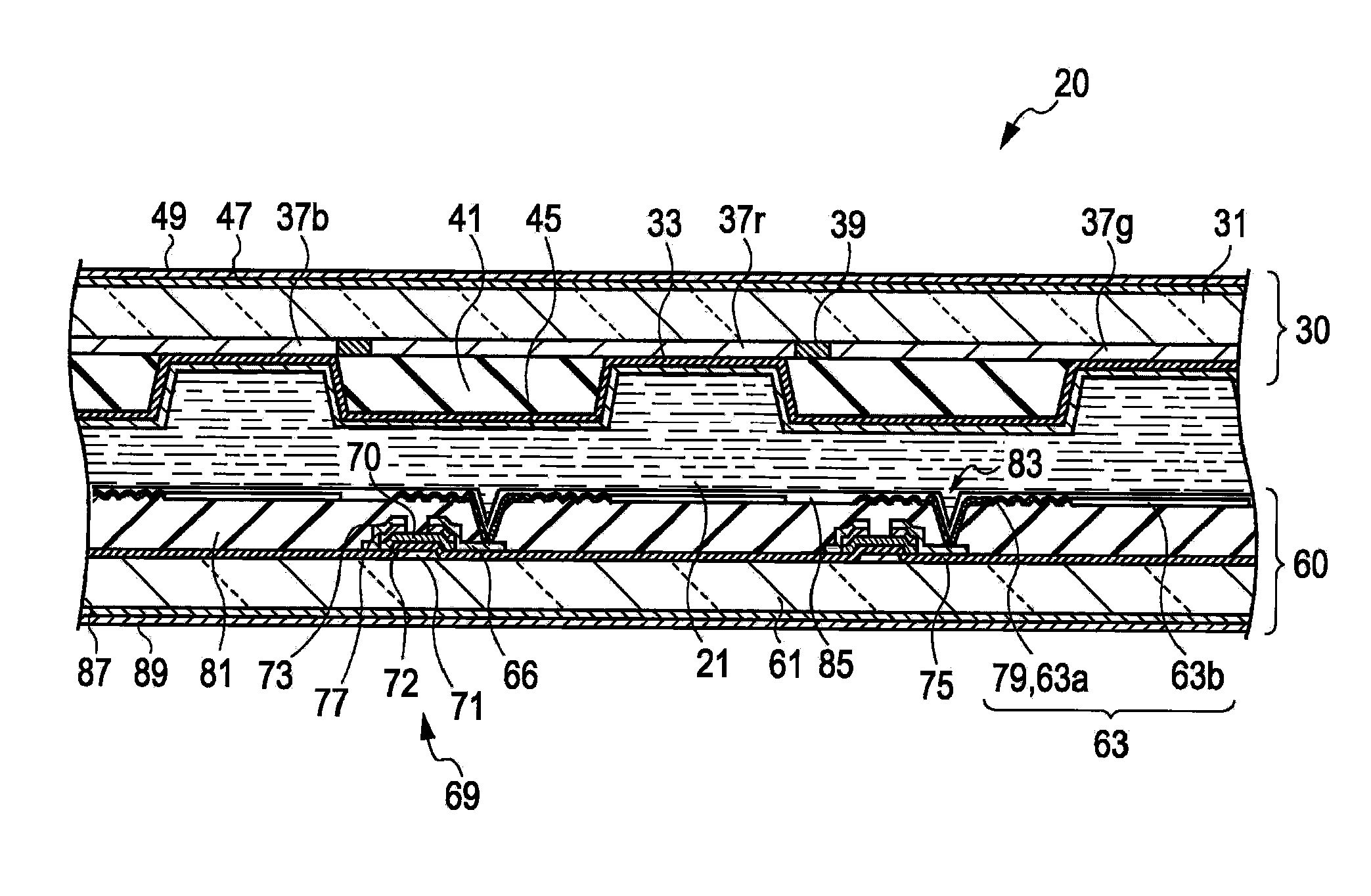
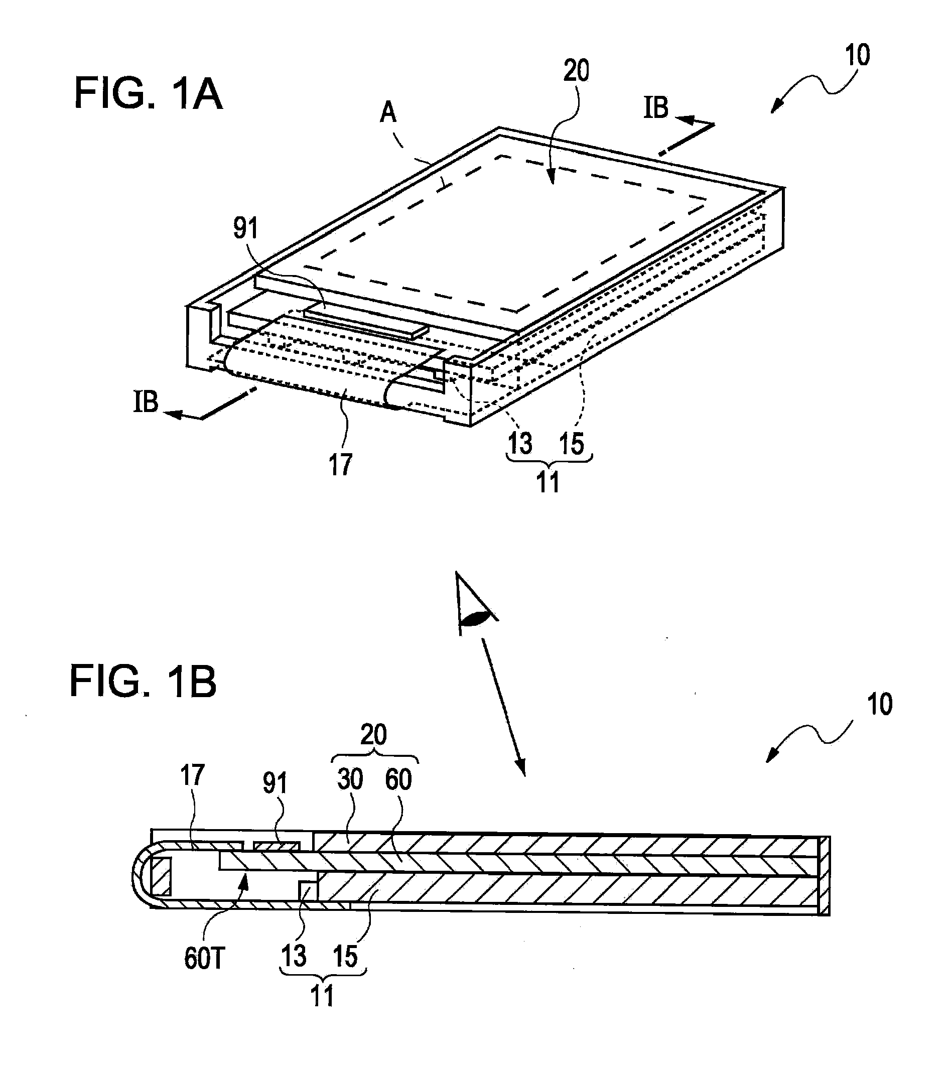
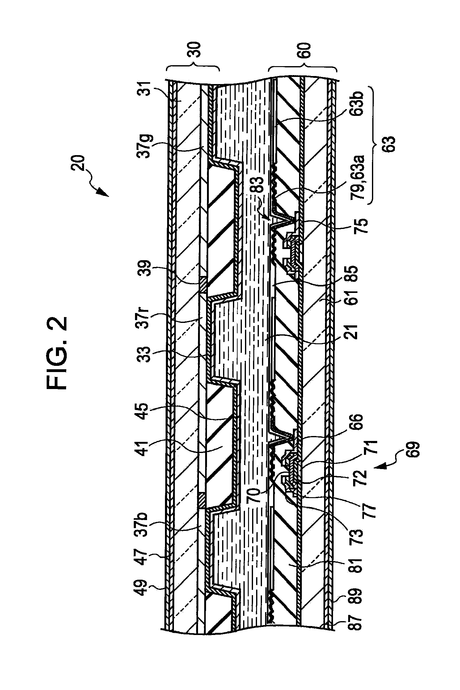
[0051]The electro-optical device will now be described with reference to FIGS. 1 to 10. The electro-optical device is not limited to an active matrix liquid crystal display including thin-film transistors (TFTs) and may be a liquid crystal display, such as a liquid crystal display including thin-film diodes (TFDs) or a passive matrix liquid crystal display, including a color filter.

[0052]1. Configuration of Electro-Optical Device

[...

second embodiment

[0117]A second embodiment of the present invention provides a method for manufacturing the electro-optical device 10 according to the first embodiment.

[0118]The method is characterized in that the color layers of different colors are sequentially formed such that the color layers of two or more colors are arranged in at least one of the subpixel region in each pixel so as not to overlap with each other in plan view.

[0119]The method will now be described in detail with reference to FIGS. 11 to 13.

[0120]1. Preparation of Element Substrate

[0121]The element substrate 60 can be prepared by a known process. The following components are formed above the second base plate 61 made of, for example, glass: the TFTs 69, the gate bus lines, the source bus lines, the external connection terminals, the pixel electrodes 63, and the like. The second alignment layer 85 made of polyimide is provided over the pixel electrodes 63. The element substrate 60 including various electric lines and conductive ...

third embodiment

[0141]A third embodiment of the present invention provides an electro-optical device which is similar to that according to the first embodiment except that one pixel includes subpixel regions including color layers of two or more colors and subpixel regions including color layers of a single color and the number of the subpixel regions present in the pixel is greater than or equal to the number of color resists for forming a color filter.

[0142]The color filter, which is the difference between the electro-optical device of this embodiment and that of the first embodiment, will now be described in detail.

[0143]The color filter used in this embodiment, as well as that used in the first embodiment, includes a plurality of color layers of different additive colors such as red, green, and blue.

[0144]With reference to FIGS. 14 to 17, at least two of each first color layer 37R, each second color layer 37G, and each third color layer 37B are arranged in at least one of subpixel regions so as...


PUM

PropertyMeasurementUnit
visible wavelengthaaaaaaaaaa
peak wavelengthaaaaaaaaaa

Abstract

An electro-optical device includes a plurality of subpixel regions forming a display field and a color filter including a plurality of color layers of which at least one is of an additive primary color. The color layers have different color hues and at least two of the color layers are arranged in at least one of the subpixel regions so as not to overlap with each other in plan view. A method for manufacturing the electro-optical device includes forming the color layers such that at least two of the color layers are arranged in at least one of the subpixel regions so as not to overlap with each other in plan view. An electronic apparatus includes the electro-optical device.

Description

[0001]The entire disclosure of Japanese Patent Application No. 2006-149321, filed May 30, 2006 is expressly incorporated by reference herein.BACKGROUND[0002]1. Technical Field[0003]The present invention relates to electro-optical devices, methods for manufacturing such electro-optical devices, and electronic apparatuses. The present invention particularly relates to an electro-optical device including a color filter including color layers of additive primary colors, a method for manufacturing such an electro-optical device, an electronic apparatus including such an electro-optical device.[0004]2. Related Art[0005]Liquid crystal displays are examples of known electro-optical devices for displaying images. The liquid crystal displays each include a plurality of subpixel regions opposed to electrodes. In the liquid crystal displays, light passing through liquid crystal materials present in the subpixel regions is modulated in such a manner that the subpixel regions are turned on or off...

Claims


Application Information

Patent Timeline
Patent Type & Authority Applications(United States)
IPC IPC(8): G02F1/1335
CPCG02F1/133514H01L27/322G02F2201/52G02F1/133516H10K59/38G02F1/1335
Inventor WACHI, REIKO
Owner JAPAN DISPLAY WEST
Why Eureka
Try Eureka