Printed circuit board with coextensive electrical connectors and contact pad areas

a printed circuit board and electrical connector technology, applied in the direction of electrical apparatus construction details, sustainable manufacturing/processing, final product manufacturing, etc., can solve the problems of large contact pads on substrates, blind and buried vias, and insufficient surface area of single-layer pcb to affect the required signal and voltage (power and ground) transfer, etc., to reduce the number of layers required and ease the restriction on the definition of tra

Active Publication Date: 2007-12-13
SANDISK TECH LLC
View PDF6 Cites 24 Cited by
  • Summary
  • Abstract
  • Description
  • Claims
  • Application Information

AI Technical Summary

Benefits of technology

[0012]Altering the shape of the contact pads to include voids that allow electrical connectors to be provided in the area of the contact pads eases the restrictions on the definition of the trace and via layout. Moreover, altering the shape of the contact pads to include voids allowing vias to be provided in the area of the contact pads increases the number of vias which may be formed through the PCB. This easing of the restrictions in defining the trace and via layout, as well as the increase in the number of vias which may be formed through the PCB may allow a reduction in the number of layers required in the PCB.

Problems solved by technology

Although it is known to form conductance patterns with very fine electrical traces, owing to the number of connections required on modem-day PCBs, there may not be enough surface area in a single-layered PCB to affect the required signal and voltage (power and ground) transfer.
A problem with this approach is that substrates often include large contact pads for receiving surface mounted components.
Blind and buried vias are, however, difficult to fabricate and add time and expense to the substrate manufacturing process.

Method used


Image

  • Printed circuit board with coextensive electrical connectors and contact pad areas
  • Printed circuit board with coextensive electrical connectors and contact pad areas
  • Printed circuit board with coextensive electrical connectors and contact pad areas

Examples


Embodiment Construction

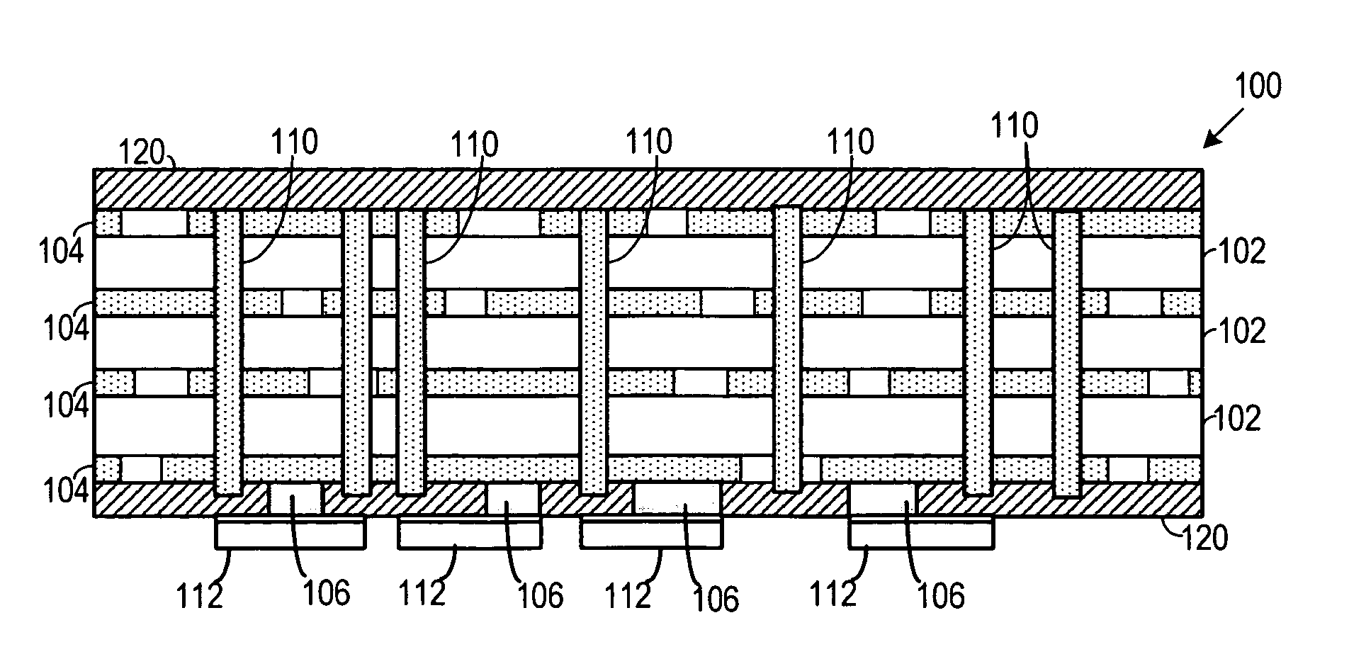
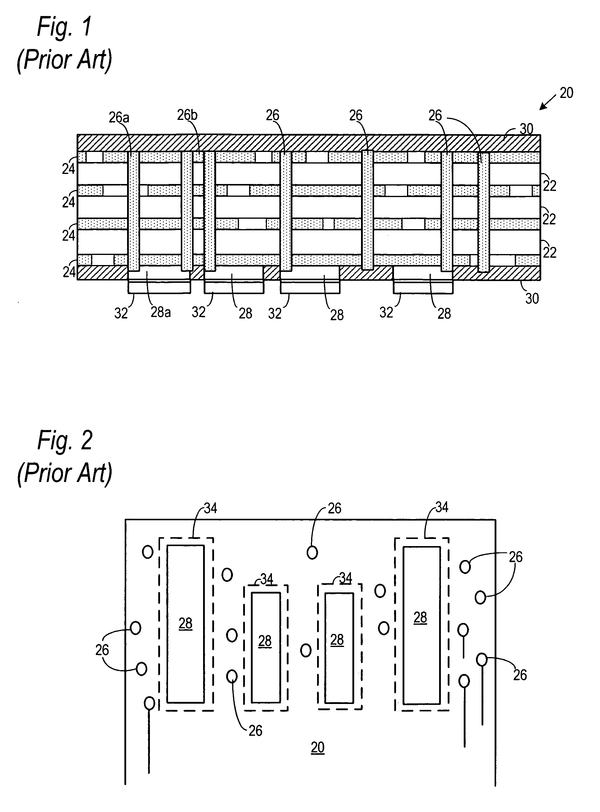
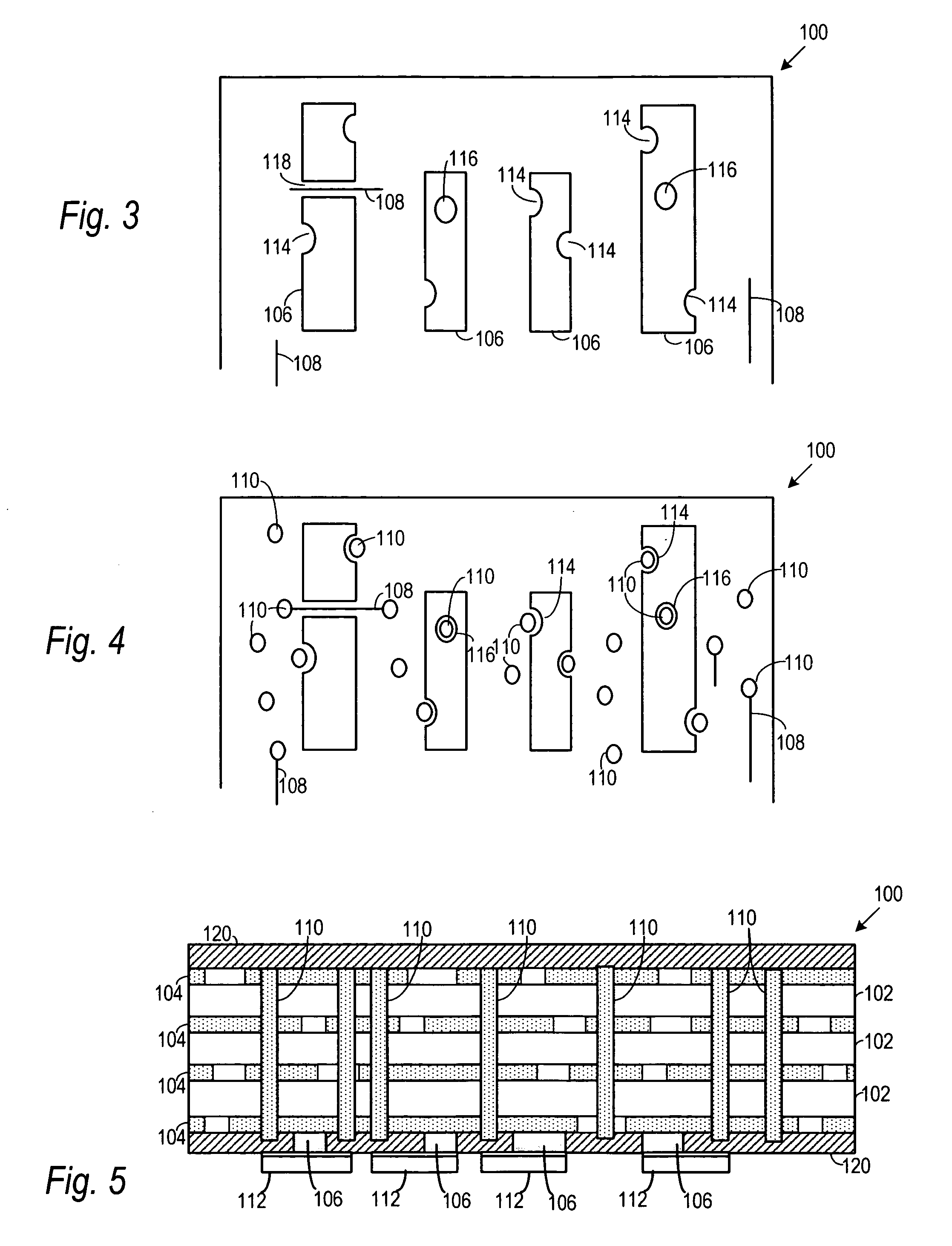
[0035]Embodiments of the invention will now be described with reference to FIGS. 3 through 21 which relate to a printed circuit board having coextensive electrical connectors and contact pad areas. It is understood that the present invention may be embodied in many different forms and should not be construed as being limited to the embodiments set forth herein. Rather, these embodiments are provided so that this disclosure will be thorough and complete and will fully convey the invention to those skilled in the art. Indeed, the invention is intended to cover alternatives, modifications and equivalents of these embodiments, which are included within the scope and spirit of the invention as defined by the appended claims. Furthermore, in the following detailed description of the present invention, numerous specific details are set forth in order to provide a thorough understanding of the present invention. However, it will be clear to those of ordinary skill in the art that the presen...


PUM


Abstract

A printed circuit board is disclosed having coextensive electrical connectors and contact pad areas. Areas of the contact pads where the traces and / or vias are located may be etched away to ensure electrical isolation between the traces, vias and contact pads.

Description

BACKGROUND OF THE INVENTION[0001]1. Field of the Invention[0002]Embodiments of the present invention relate to a printed circuit board having coextensive electrical connectors and contact pad areas.[0003]2. Description of the Related Art[0004]The strong growth in demand for portable consumer electronics is driving the need for high-capacity storage devices. Non-volatile semiconductor memory devices, such as flash memory storage cards and devices, are becoming widely used to meet the ever-growing demands on digital information storage and exchange. Their portability, versatility and rugged design, along with their high reliability and large capacity, have made such memory devices ideal for use in a wide variety of electronic devices, including for example digital cameras, digital music players, video game consoles, PDAs and cellular telephones.[0005]Flash memory devices may include a printed circuit board (“PCB”) for supporting electronic components and / or for transmitting electrical...

Claims


Application Information

Patent Timeline
Patent Type & Authority Applications(United States)
IPC IPC(8): H01L23/12H01L23/48
CPCH05K1/111H05K1/115H05K3/429H05K2201/09381H05K2201/094H05K2201/09663H01L2924/0002H05K2201/0969H05K2201/10689H01L2924/00H05K2201/10159Y02P70/50H05K1/0298H05K1/181H05K3/4038H05K2201/0195H05K2201/0338
Inventor LIAO, CHIH-CHINCHEN, HAN-SHIAOCHIU, CHIN-TIENWANG, KEN JIAN MINGYU, CHEEMENTAKIAR, HEM
Owner SANDISK TECH LLC
Why Eureka
Try Eureka