

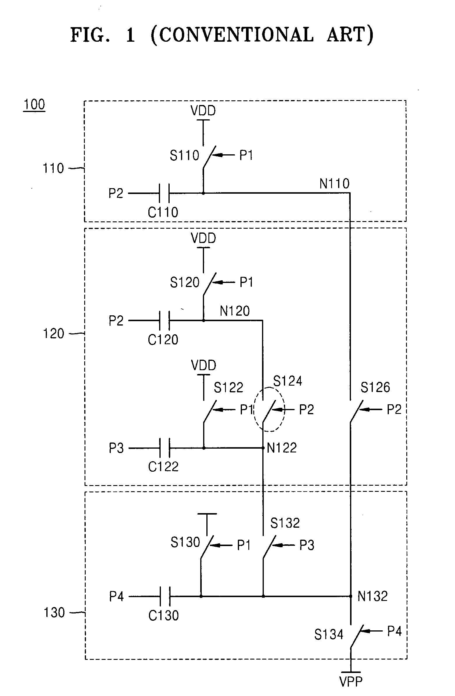
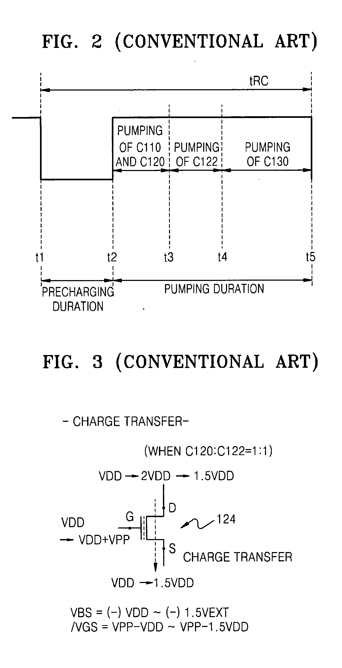
High-voltage generating circuit including charge transfer switching circuit for selectively controlling body bias voltage of charge transfer device
a high-voltage generating circuit and switching circuit technology, applied in electronic switching, digital storage, instruments, etc., can solve the problems of significant reduction of charge transfer efficiency, and achieve the effect of increasing the efficiency of charge transfer during charge transfer, reducing and/or preventing a backflow of charges
- Summary
- Abstract
- Description
- Claims
- Application Information
AI Technical Summary
Benefits of technology
Problems solved by technology
Method used
Image

Examples
Embodiment Construction
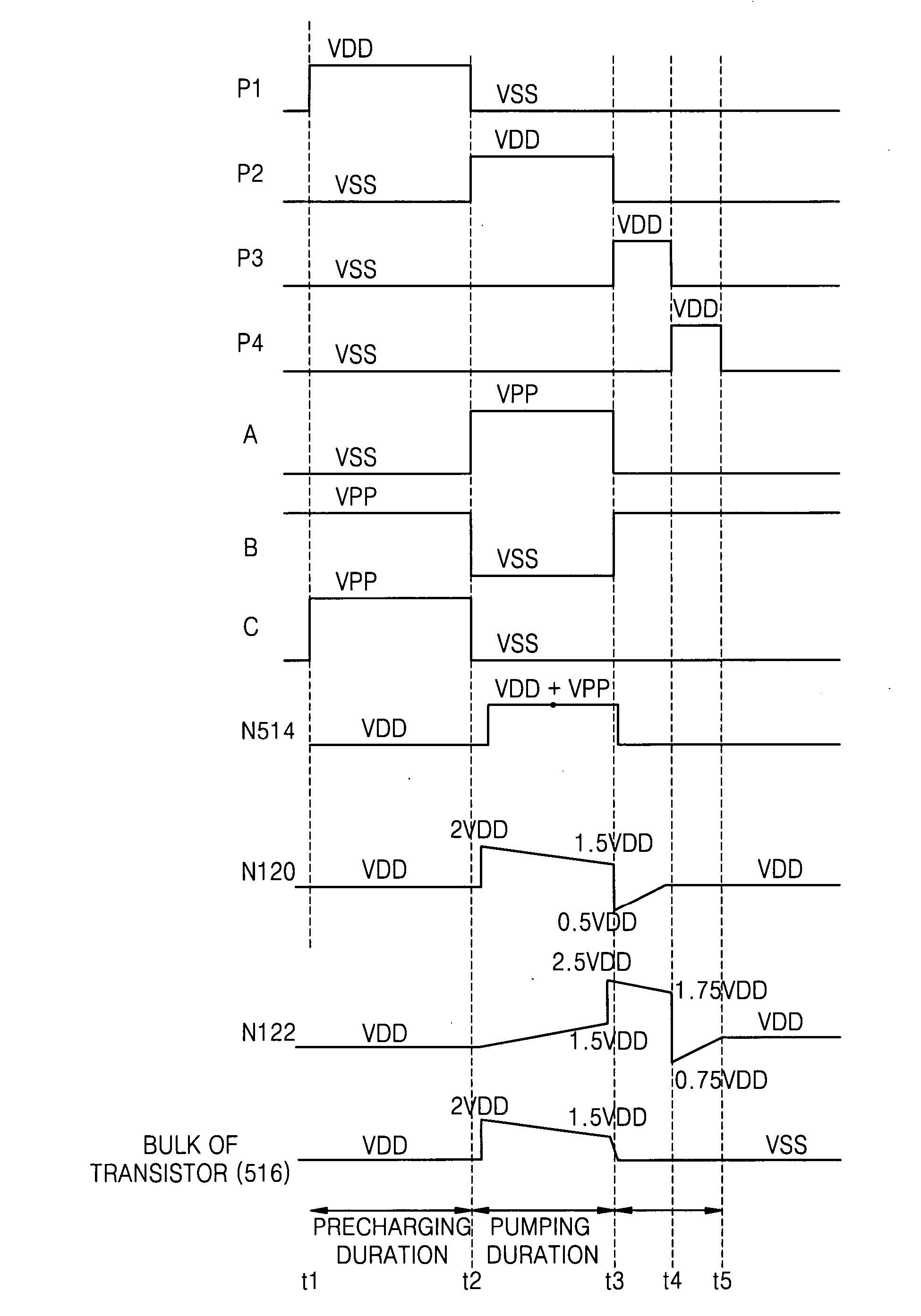
[0034] Various example embodiments will now be described more fully with reference to the accompanying drawings. However, specific structural and functional details disclosed herein are merely representative for purposes of describing example embodiments, and one skilled in the art will appreciate that example embodiments may be embodied in many alternate forms and should not be construed as limited to only the embodiments set forth herein.
[0035] It should be understood that, although the terms first, second, etc. may be used herein to describe various elements, these elements should not be limited by these terms. These terms are only used to distinguish one element from another. For example, a first element could be termed a second element, and, similarly, a second element could be termed a first element, without departing from the scope of the example embodiments. As used herein, the term “and / or” includes any and all combinations of one or more of the associated listed items.
[0...
PUM
 Abstract
Description
Claims
Application Information