Wiring module, method and apparatus for manufacturing wiring module

a wiring module and wiring module technology, applied in the direction of resistive material coating, solid-state device, metallic material coating process, etc., can solve the problems of increasing mounting cost and severely limited application of conventional mounting methods, so as to reduce the number of manufacturing steps, reduce time and cost, and improve reliability

Active Publication Date: 2007-12-13
CANON KK
View PDF4 Cites 15 Cited by
  • Summary
  • Abstract
  • Description
  • Claims
  • Application Information

AI Technical Summary

Benefits of technology

[0008]An object of the present invention is to provide a method for manufacturing an electronic circuit part module which method enables dense mounting and a reduction in wiring distance.
[0014]The present invention enables the wiring module to be manufactured using a reduced number of manufacturing steps. This enables a substantial reduction in the time and cost required for the manufacture and improves reliability. Further, electronic circuit parts can be freely arranged three-dimensionally in the wiring module and wires can be freely drawn. The arrangement density and wiring density of the electronic circuit parts can thus be increased. This contributes to increasing the speed of electronic circuit operations.

Problems solved by technology

However, the presently proposed method for three-dimensionally arranging electronic circuit parts is effective only for stacking of a plurality of electronic circuit parts of the same shape such as memory chips.
Disadvantageously, this method also increases mounting costs.
Thus, the application of the conventional mounting methods is severely limited.

Method used


Image

  • Wiring module, method and apparatus for manufacturing wiring module
  • Wiring module, method and apparatus for manufacturing wiring module
  • Wiring module, method and apparatus for manufacturing wiring module

Examples


first example

[0057]Now, with reference to FIGS. 3 to 6, a specific description will be given of a process of actually manufacturing a wiring module in accordance with the above embodiment.

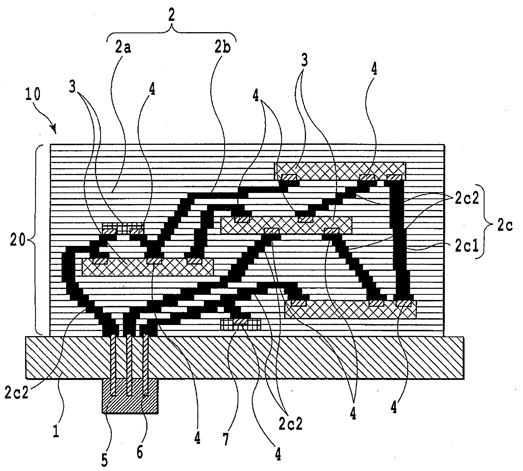
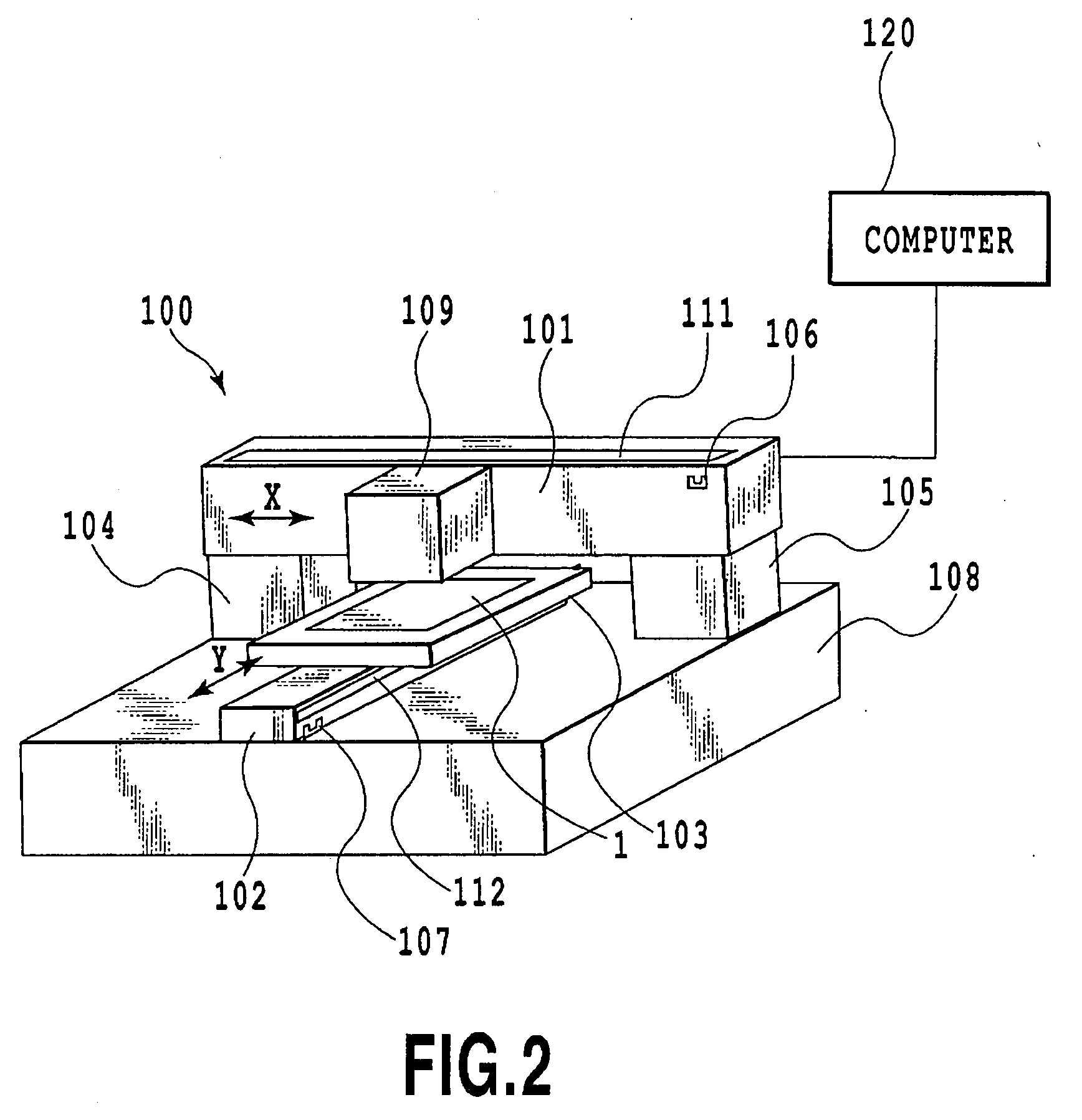
[0058]Description will be given of an example in which the wiring module shown in FIG. 1 is manufactured by using the wiring module manufacturing apparatus 100, described with reference to FIG. 2, form wiring patterns 2 on the base material 1.

[0059]In this case, the base material 1 was a ceramics plate of thickness 2 mm mainly consisting of alumina, which offers an insulating property and a high heat resistance. The connector 5 is pre-fixed to the base material 1 to electrically connect the wiring module to an external device.

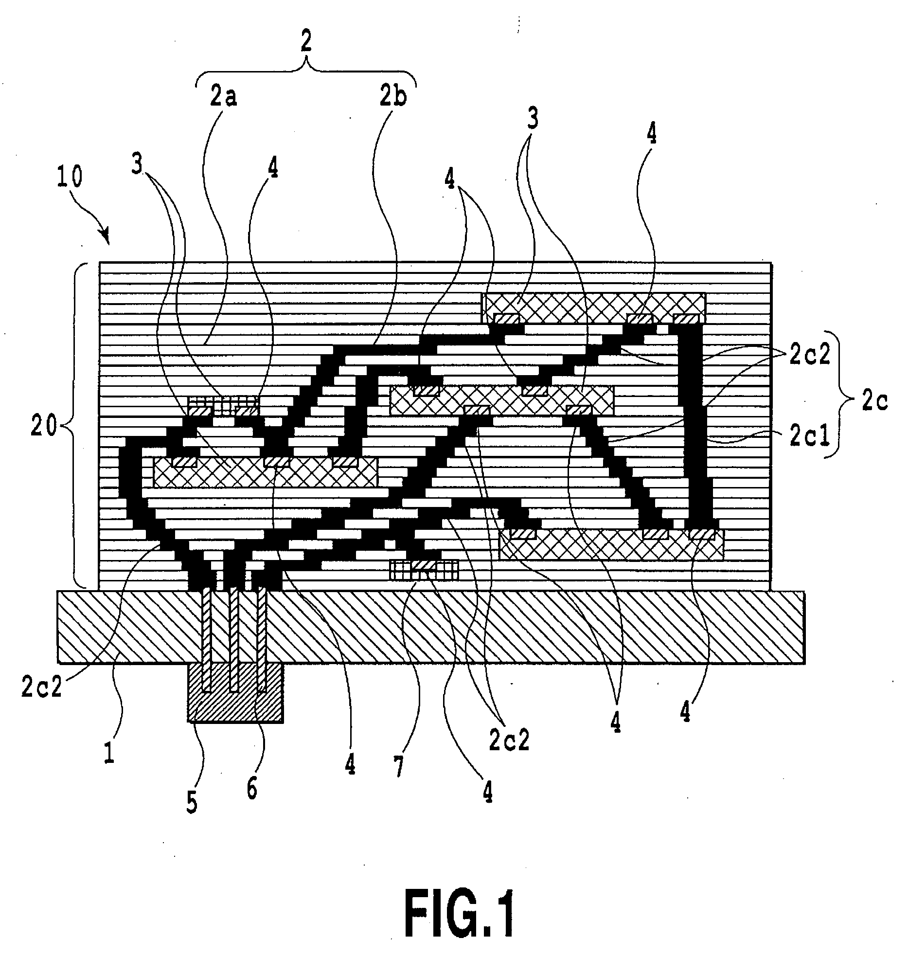
[0060]FIG. 3 shows that a first layer of the wiring pattern 2 is being formed on the base material 1.

[0061]In the figure, reference numeral 11 denotes the liquid ejecting head mounted on the carriage 109. The liquid ejecting head 11 has a plurality of nozzles 12 (first ejecting portions) 1...

second example

[0066]Now, a second example of the present invention will be described with reference to FIGS. 7 and 8.

[0067]In the second example, a wiring module is manufactured by forming wiring patterns on a flexible temporary base material 15 that is different from the base material 1, finally formed into a wiring module, and then transferring the wiring patterns to the base material 1.

[0068]FIG. 7 shows that a layer forming step has been executed to form wiring patterns 2 on the temporary base material 15. The temporary base material 15 was a polyimide film of thickness 100 μm, which is flexible and offers a high heat resistance. Wiring patterns 2 were formed on the temporary base material 15 using the wiring module manufacturing apparatus 100, described with reference to FIG. 2, as is the case with the first example. FIG. 7 shows that one layer of the wiring pattern 2 has been formed on the temporary base material 15. However, plural layers of the wiring pattern 2 may be formed on the tempor...


PUM

PropertyMeasurementUnit
thicknessaaaaaaaaaa
thicknessaaaaaaaaaa
widthaaaaaaaaaa

Abstract

An object of the present invention is to provide a wiring module that enables dense mounting and a reduction in wiring distance. The wiring module in accordance with the present invention includes a base material, a plurality of electronic circuit parts, insulating portions, and conductive portions connected to the electronic circuit parts, the plurality of electronic circuit parts, the insulating portions, and the conductive portions being integrally held on the base material. Wires are composed of a stack of the conductive portions and extend in a direction crossing a surface of the base material and in a direction crossing a direction perpendicular to the base material surface to electrically connect the plurality of electronic circuit parts together.

Description

BACKGROUND OF THE INVENTION[0001]1. Field of the Invention[0002]The present invention relates to methods for manufacturing wiring modules provided with electronic circuit parts used in electronic instruments, electric instruments, computers, communication instruments, and the like.[0003]2. Description of the Related Arts[0004]In general, wiring modules are produced by mounting semiconductors such as LSIs, various electronic circuit parts, and the like on a printed circuit board. These wiring modules are used in electronic instruments such as computers. Various printed circuit boards in which the electronic circuit parts are mounted are known, including those formed using ceramics, those formed using a composite material of a reinforcing material such as glass fibers and a synthetic resin such as an epoxy resin, and those formed using a flexible film such as a polyester resin or an aramid resin. With respect to the number of circuit layers on the same surface of a double-faced board ...

Claims


Application Information

Patent Timeline
Patent Type & Authority Applications(United States)
IPC IPC(8): H01L23/00
CPCH01L21/6835Y10T29/53174H01L24/24H01L24/25H01L24/76H01L24/82H01L25/0652H01L25/16H01L2221/68345H01L2221/68363H01L2224/24011H01L2224/24137H01L2224/24145H01L2224/2518H01L2224/76155H01L2924/01012H01L2924/01013H01L2924/0102H01L2924/01029H01L2924/01056H01L2924/14H01L2924/19041H01L2924/19043H05K1/185H05K3/1241H05K3/4069H05K3/465H05K3/4664H05K2201/09845H05K2201/10674H05K2203/0568H01L2924/01006H01L2924/01024H01L2924/01033H01L2924/01047H01L2924/014H01L2224/82102H01L2224/24105H01L23/5389
Inventor YAMAGUCHI, NOBUHITOTSURUOKA, YUJIMORI, TAKASHIFURUKAWA, MASAOKAMIYA, SEIICHI
Owner CANON KK
Why Eureka
Try Eureka