Process chamber for dielectric gapfill

a dielectric gap and process chamber technology, applied in the coating process, chemical vapor deposition coating, coating, etc., can solve the problems of high aspect ratio gap, difficult to fill tall and narrow gap, and difficult to separate the gaps of the elements

Inactive Publication Date: 2007-12-20
APPLIED MATERIALS INC
View PDF13 Cites 252 Cited by
  • Summary
  • Abstract
  • Description
  • Claims
  • Application Information

AI Technical Summary

Benefits of technology

[0008] Embodiments of the invention include systems to form a dielectric layer on a substrate from a plasma of dielectric precursors. The systems may include a deposition chamber, a substrate stage in the deposition chamber to hold the substrate, and a remote plasma generating system coupled to the deposition chamber, where the plasma generating system is used to generate a dielectric precursor having one or more reactive radicals. The system may also include a precursor distribution system that includes at l...

Problems solved by technology

As integrated circuit chipmakers continue increasing the density of circuit elements on each chip, filling the gaps that separate those elements becomes more challenging.
It is more difficult to fill a tall and narrow gap (i.e., a high aspect ratio gap) with a uniform film of dielectric material than a shallow and wide gap (i.e., a low aspect ratio gap).
One commonly encountered difficulty with filling high aspect ratio gaps is the formation of voids.
Often the dielectric material will close the top before the gap has been completely filled, leaving a void.
Even when the top of the gap does not close prematurely, the uneven growth rate of the dielectric film down the sidewalls of the gap can create a weak seam...

Method used


Image

  • Process chamber for dielectric gapfill
  • Process chamber for dielectric gapfill
  • Process chamber for dielectric gapfill

Examples


Embodiment Construction

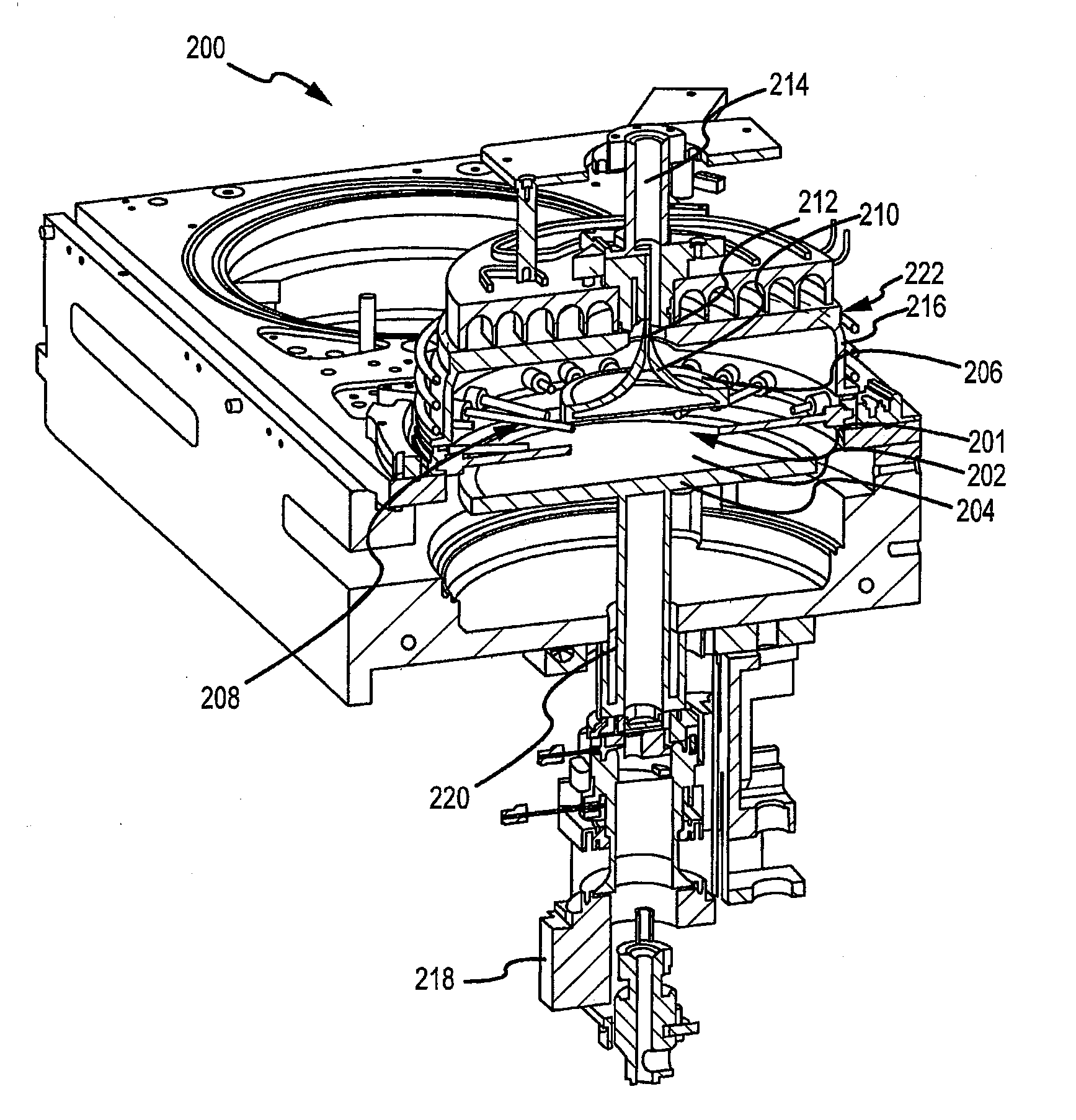
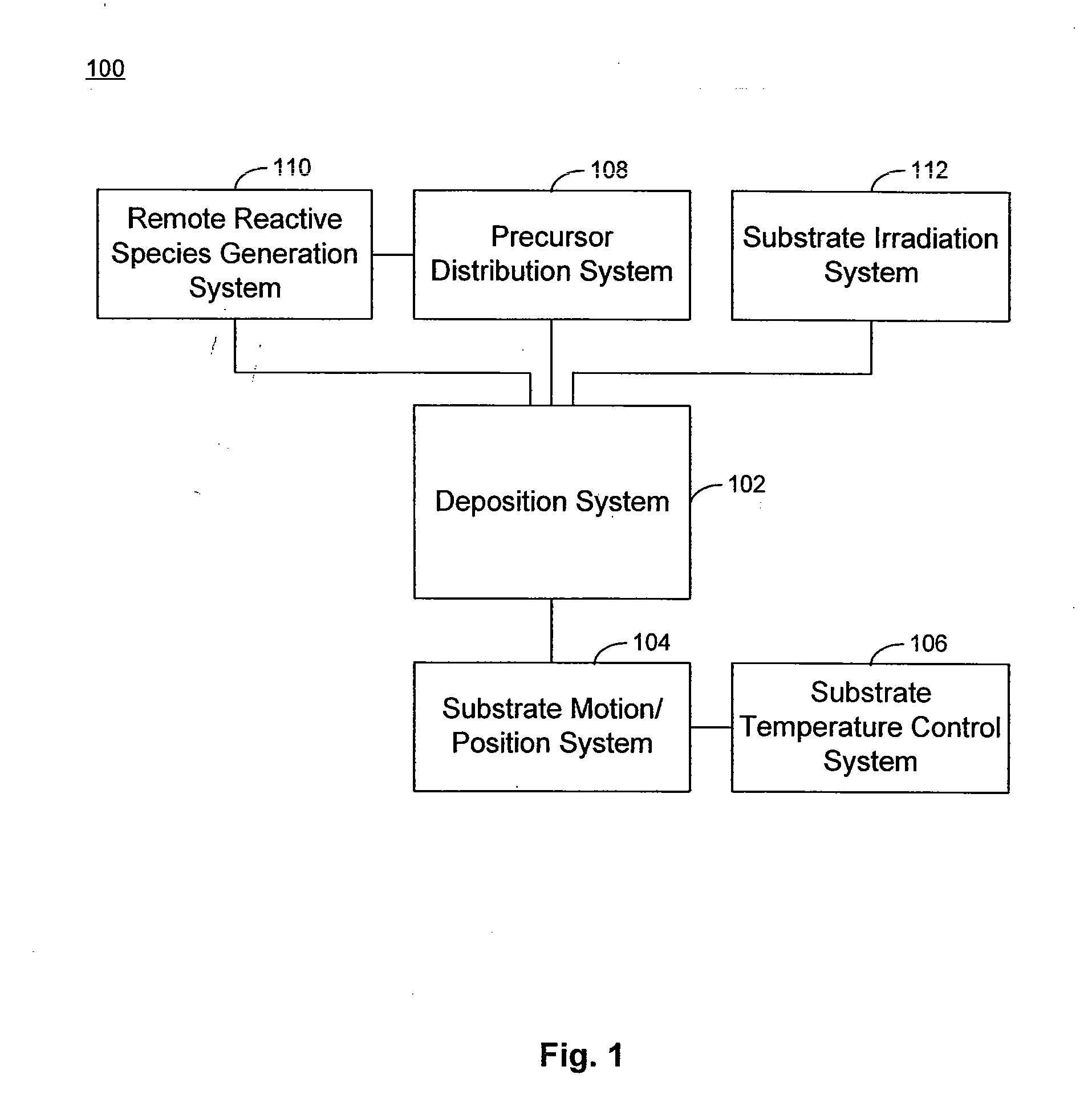
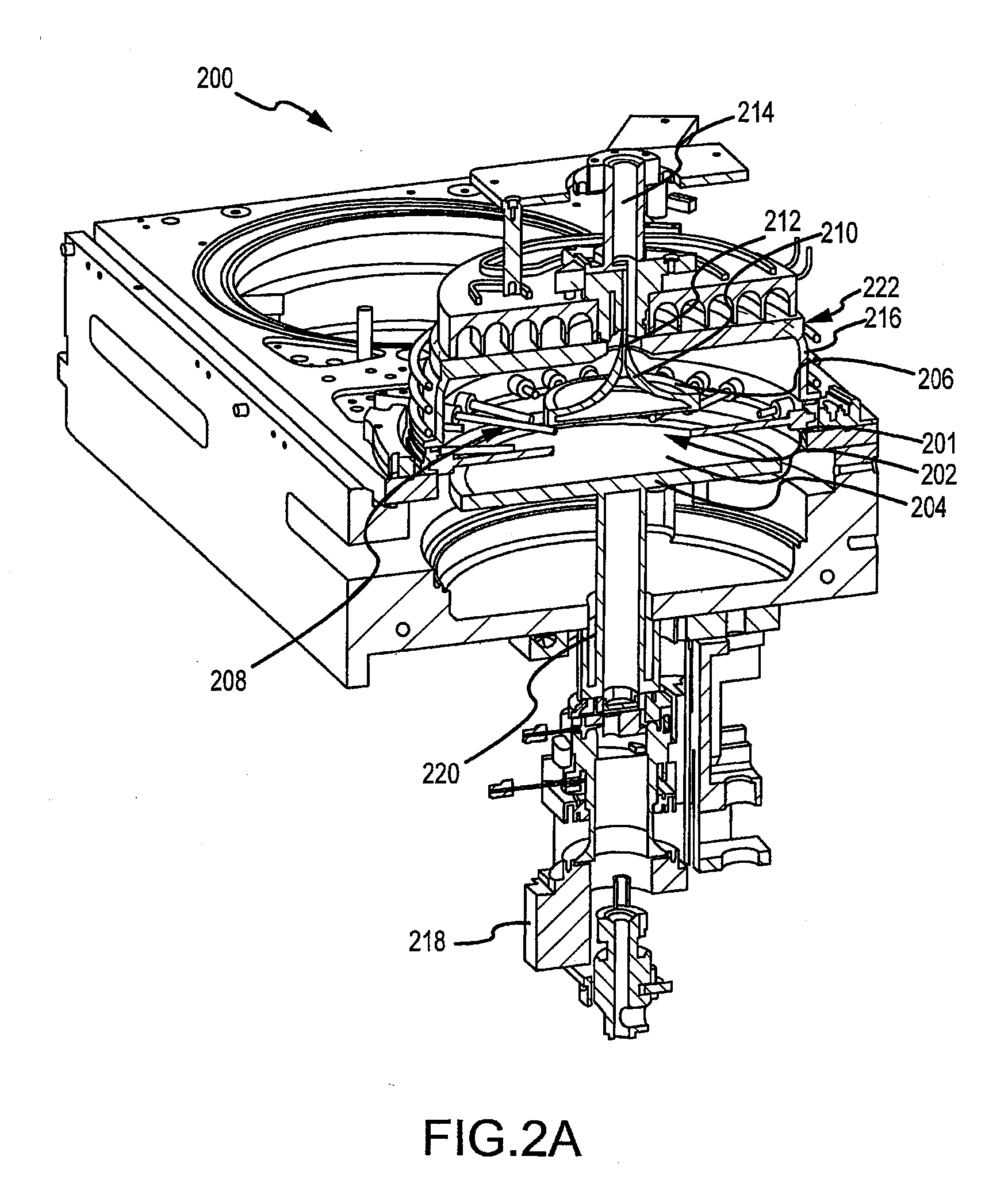
[0039] Systems are described for depositing a flowable CVD dielectric film on a substrate. These dielectric films may be used for STI, IMD, ILD, OCS, and other applications. The systems may include a reactive species generation system that supplies reactive radical species to a deposition chamber, where the species chemically react with other deposition precursors and form a flowable film of dielectric on a deposition surface of the substrate. For example the system may form a layer on a substrate from excited oxygen by a remote plasma source and organo-silane types of precursors. The systems may also include substrate temperature control systems that can both heat and cool the substrate during a deposition. For example, the flowable oxide film may be deposited on the substrate surface at low temperature (e.g., less that 100° C.) which is maintained by cooling the substrate during the deposition. Following the film deposition, the temperature control system may heat the substrate to...


PUM

PropertyMeasurementUnit
Temperatureaaaaaaaaaa

Abstract

A system to form a dielectric layer on a substrate from a plasma of dielectric precursors is described. The system may include a deposition chamber, a substrate stage in the deposition chamber to hold the substrate, and a remote plasma generating system coupled to the deposition chamber, where the plasma generating system is used to generate a dielectric precursor having one or more reactive radicals. The system may also include a radiative heating system to heat the substrate that includes at least one light source, where at least some of the light emitted from the light source travels through the top side of the deposition chamber before reaching the substrate. The system may also include a precursor distribution system to introduce the reactive radical precursor and additional dielectric precursors to the deposition chamber. An in-situ plasma generating system may also be included to generate the plasma in the deposition chamber from the dielectric precursors supplied to the deposition chamber.

Description

CROSS-REFERENCES TO RELATED APPLICATIONS [0001] This application claims the benefit of U.S. Provisional Application No. 60 / 803,499 filed May 30, 2006. This application is also related to co-assigned U.S. Provisional Application No. 60 / 803,489 by Munro et al, filed May 30, 2006 and titled “A METHOD FOR DEPOSITING AND CURING LOW-K FILMS FOR GAPFILL AND CONFORMAL FILM APPLICATIONS”. This application is also related to co-assigned U.S. Provisional App. No. 60 / 803,493, by Ingle et al, filed May 30, 2006 and titled “CHEMICAL VAPOR DEPOSITION OF HIGH QUALITY FLOW-LIKE SILICON DIOXIDE USING A SILICON CONTAINING PRECURSOR AND ATOMIC OXYGEN”. This application is also related to U.S. Provisional Application No. 60 / 803,481, by Chen et al, filed May 30, 2006 and titled “A NOVEL DEPOSITION-PLASMA CURE CYCLE PROCESS TO ENHANCE FILM QUALITY OF SILICON DIOXIDE”. The entire contents of the priority U.S. Provisional patent application and the related applications are herein incorporated by reference f...

Claims


Application Information

Patent Timeline
IPC IPC(8): C23C16/452
CPCC23C16/452C23C16/45565C23C16/45574C23C16/46H01L21/67115
Inventor LUBOMIRSKY, DMITRYLIANG, QIWEIPARK, SOONAMCHUC, KIENYIEH, ELLIE
Owner APPLIED MATERIALS INC
Why Eureka
Try Eureka