Via layout with via groups placed in interlocked arrangement

a technology of interlocked arrangement and via layout, which is applied in the direction of semiconductor devices, semiconductor/solid-state device details, electrical apparatus, etc., can solve the problems of cracking failure to allow the integrated circuit to underlie the bond pad, and deformation of the imd layer, so as to improve the critical dimension uniformity or thickness uniformity

Active Publication Date: 2007-12-20
TAIWAN SEMICON MFG CO LTD
View PDF7 Cites 152 Cited by
  • Summary
  • Abstract
  • Description
  • Claims
  • Application Information

AI Technical Summary

Benefits of technology

[0005]Embodiments of the present invention include a via layout with via groups placed in an interlocked arrangement for bond pad structures in order to avoid a straight open path existed along the domain boundary between two adjacent via groups. Also, embodiments of the present invention provide a dummy pattern layout with line groups placed in an interlocked arrangement around an active area or within a dummy region defined on a semiconductor substrate for improving critical dimension uniformity or thickness uniformity during chemical mechanical polishing.

Problems solved by technology

The large, exposed, surface area of IMD layer, however, surrounding the smaller regions of metal vias, can result in defect formation, as a result of the large bonding force experienced during the wire bonding tests, where the large bonding force is distributed throughout the overlying bond pad.
A significant failure mode involves cracking of the IMD layer.
Such a mesh via pattern is often formed or deposited in a manner that can't fully fill holes to provide poor coverage on intersection areas where line vias cross with each other, mainly because of a marginal photolithography process window induced by circuits under pad (CUP) layout.
In order to avoid problems in devices that could arise from non-fully filled metal vias, design rules do not allow integrated circuits to underlie the bond pad.

Method used


Image

  • Via layout with via groups placed in interlocked arrangement
  • Via layout with via groups placed in interlocked arrangement
  • Via layout with via groups placed in interlocked arrangement

Examples


Embodiment Construction

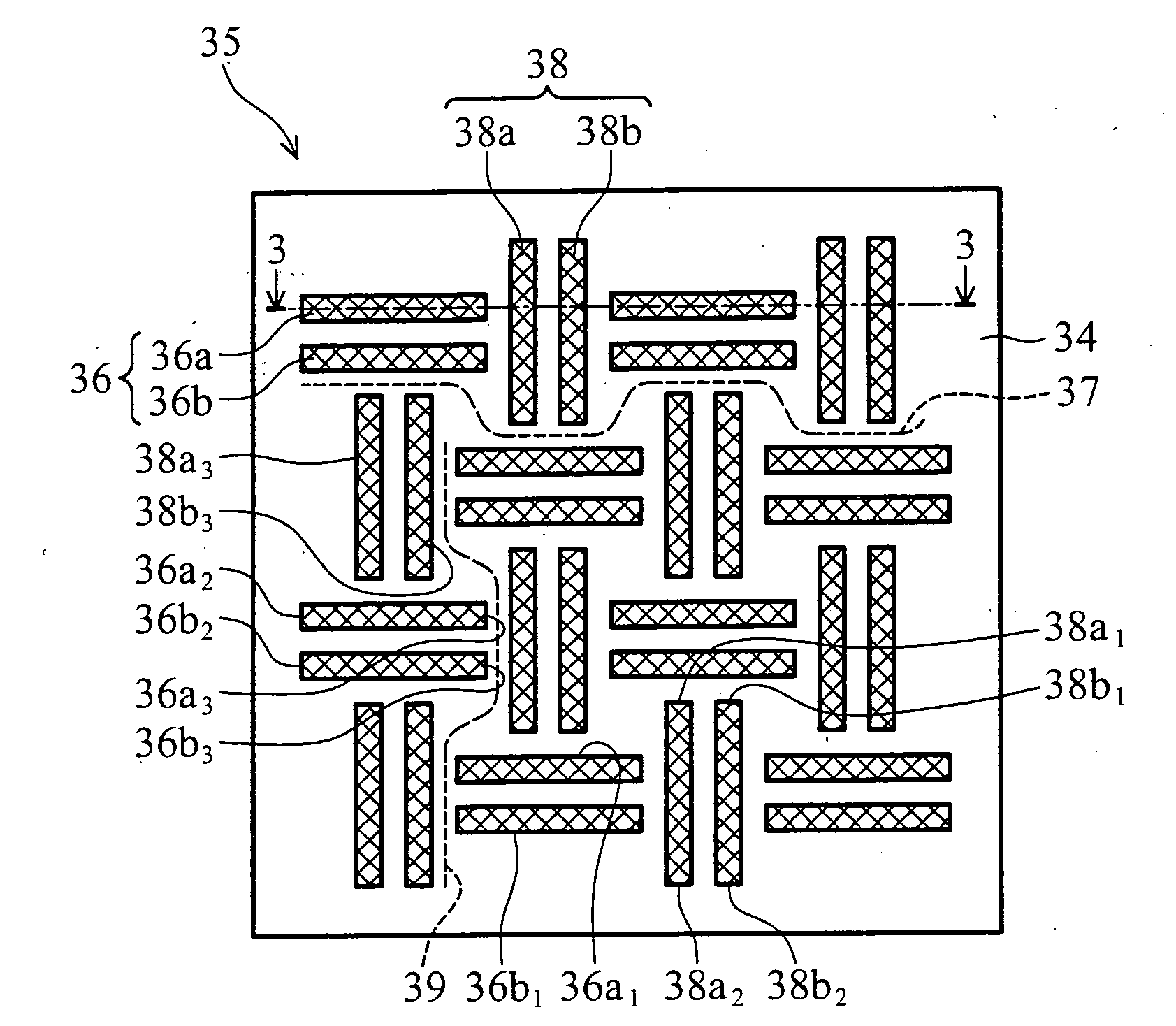
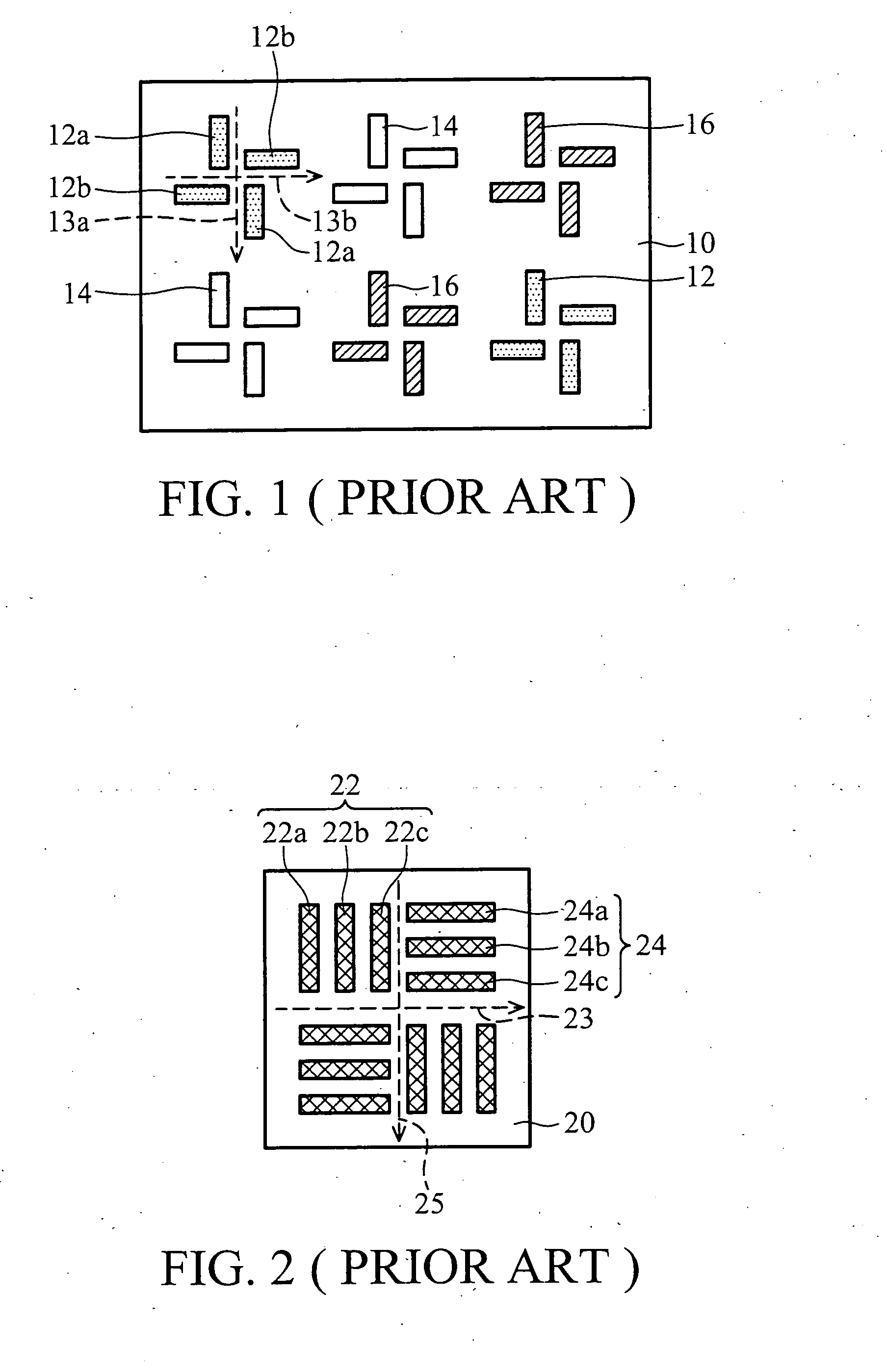
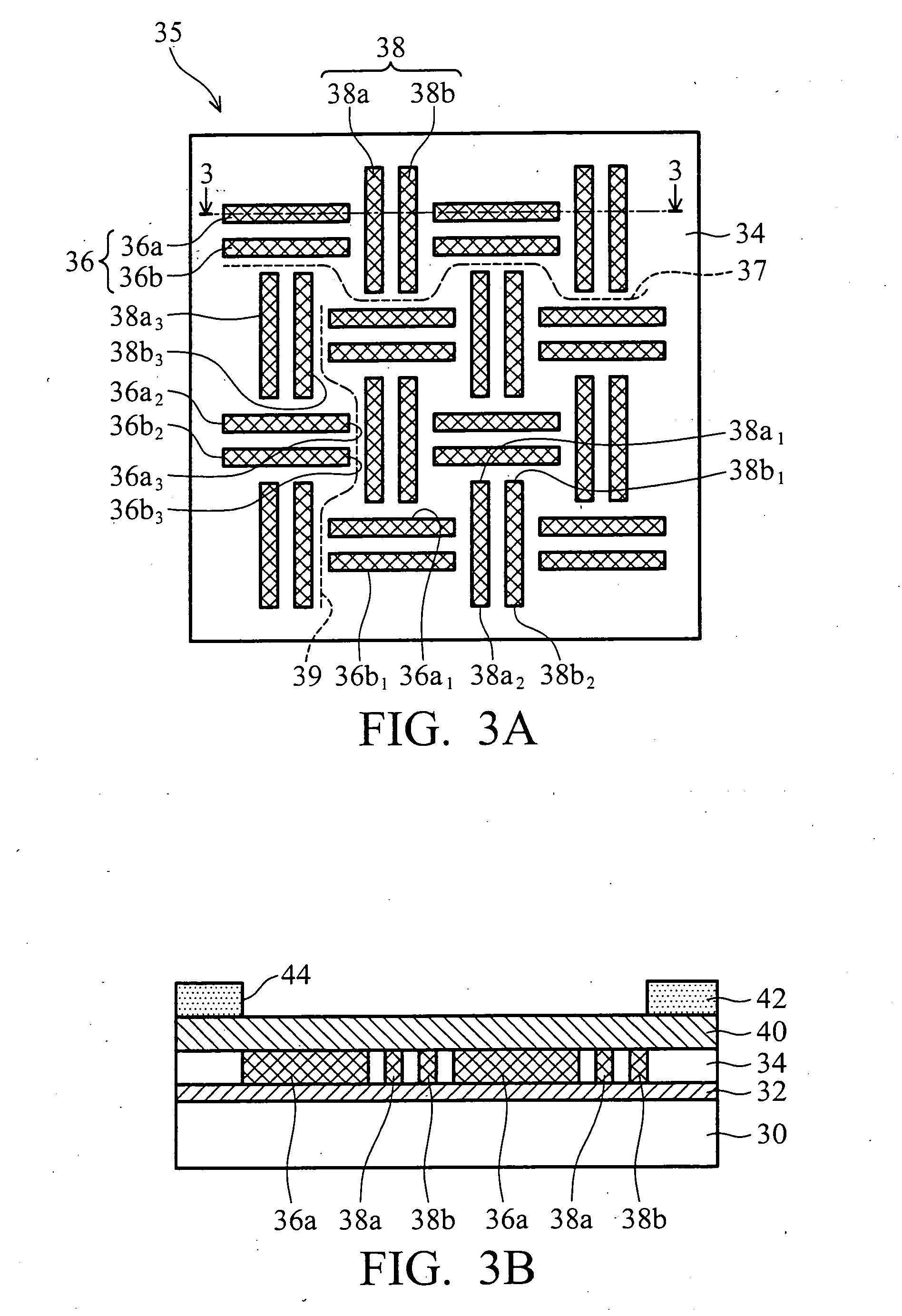
[0024]Embodiments of the present invention provide a via layout with via groups placed in an interlocked arrangement to overcome the aforementioned problems of the prior art arising from a straight open path existed along the domain boundary between the two adjacent via groups. The inventive via layout comprises at least two via groups consisting of line vias that keep a dense via density, which increases the via contact area with an overlying metal layer so as to improve adhesive results and prevent the overlying metal layer from peeling during subsequent processes (e.g., wire bonding process). The two adjacent via groups have line vias extending in different directions without generating an intersection area there between, which avoids poor via coverage. Particularly, the two adjacent via groups are arranged in an interlocked structure to avoid a straight open path existed along the domain boundary between the two adjacent via groups, which increases the toughness of the IMD layer...


PUM


Abstract

Via layout with via groups placed in an interlocked arrangement for suppressing the crack propagation along the domain boundary between the via groups. A structure has a metal via pattern located in a dielectric layer and having a first via group and a second via group adjacent to each other. The first via group has at least two first line vias extending in a first direction, and the second via group has at least two second line vias extending in a second direction. The first via group and the second via group are placed in an interlocked arrangement, and a domain boundary along the first direction or the second direction between the first via group and said second via group is not straight.

Description

TECHNICAL FIELD[0001]The present invention relates to integrated circuit structures, and particularly to a via layout with via groups placed in an interlocked arrangement for a semiconductor device.BACKGROUND[0002]Wire bonds, physically, as well as electrically, connected to underlying circuitry, of semiconductor chips, are used to connect the specific semiconductor chip to packaging elements, such as printed circuit board, or ceramic modules. Bond pads are the interfaces between the integrated circuits contained in semiconductor chips and the chip package. A large number of bond pads are required to transmit power / ground and input / output signals to the chip devices. It is thus important that reliability of bond pad should be sufficiently high to ensure the life time of the device. The general bond pad consists of metal layers separated by inter-metal dielectric (IMD) layers and metal vias passing the IMD layers for electrically connecting the metal layers. A passivation layer cover...

Claims


Application Information

Patent Timeline
Patent Type & Authority Applications(United States)
IPC IPC(8): H01L23/48
CPCH01L23/5226H01L2924/01024H01L24/05H01L2224/05093H01L2924/01005H01L2924/01012H01L2924/01013H01L2924/01014H01L2924/01015H01L2924/01022H01L2924/01025H01L2924/01029H01L2924/0103H01L2924/01032H01L2924/01033H01L2924/01038H01L2924/0104H01L2924/01049H01L2924/0105H01L2924/01073H01L2924/01074H01L2924/01078H01L2924/05042H01L2924/10329H01L2924/14H01L2924/19041H01L2924/19042H01L2924/19043H01L2924/30105H01L2924/01006H01L2924/01019H01L23/528
Inventor CHEN, JONG
Owner TAIWAN SEMICON MFG CO LTD
Why Eureka
Try Eureka