Inspection system and inspection circuit thereof, semiconductor device, display device, and method of inspecting semiconductor device

a technology of inspection circuit and inspection system, which is applied in the direction of electronic circuit testing, measurement devices, instruments, etc., can solve the problems of increasing the cost of high-speed ic, increasing the power consumption and further increasing the cost of a high-speed ic. , to achieve the effect of finer image, high serial format rate, and large number of pixels

Inactive Publication Date: 2007-12-20
NEC CORP +1
View PDF5 Cites 10 Cited by
  • Summary
  • Abstract
  • Description
  • Claims
  • Application Information

AI Technical Summary

Benefits of technology

[0015]However, in the conventional technology described above and the liquid crystal display device integrated with a drive circuit described in Patent Document 1, display data for all pixels is transferred to a liquid crystal module for each frame at a high rate in serial format. Therefore, the finer an image is and the larger the number of pixel is, the larger the transfer rate becomes. As the result of transfer at a high rate, a driver IC (integrated circuit) is also required for higher transfer rate operation, and accordingly through current etc. may be produced in a number of CMOSs (complementary metal oxide semiconductor) constituting a circuit element. Then, electric power consumption is increased due to increase in operation speed. Further, a cost of a high-speed IC is increased. Moreover, the more a number of gradation increases, the more a circuit configuration is complex and the more : a transfer rate further increases, resulting in further more power consumption and a larger cost. That is, higher-definition and higher-gradation display causes a cost and power consumption of the driver IC to be increased, which presents a problem that the number of pixel and the number of gradation are limited because the increase on power consumption and a cost of the entire system are to be suppressed.

Problems solved by technology

Then, electric power consumption is increased due to increase in operation speed.
Further, a cost of a high-speed IC is increased.
Moreover, the more a number of gradation increases, the more a circuit configuration is complex and the more : a transfer rate further increases, resulting in further more power consumption and a larger cost.
That is, higher-definition and higher-gradation display causes a cost and power consumption of the driver IC to be increased, which presents a problem that the number of pixel and the number of gradation are limited because the increase on power consumption and a cost of the entire system are to be suppressed.
Further, voltage used for each of circuit blocks on the display device substrate 101 (see FIGS. 36 and 37) is different from each other, and therefore processes corresponding to a plurality of voltages have to be used together, also resulting in a problem of a higher cost of manufacturing process.
Moreover, in this liquid crystal display device integrated with a drive circuit, the controller IC 102 and an interface IC 114 (see FIGS. 36 and 37) are provided outside the display device substrate, also presenting a problem that a display device cannot be miniaturized.

Method used


Image

  • Inspection system and inspection circuit thereof, semiconductor device, display device, and method of inspecting semiconductor device
  • Inspection system and inspection circuit thereof, semiconductor device, display device, and method of inspecting semiconductor device
  • Inspection system and inspection circuit thereof, semiconductor device, display device, and method of inspecting semiconductor device

Examples


example 1

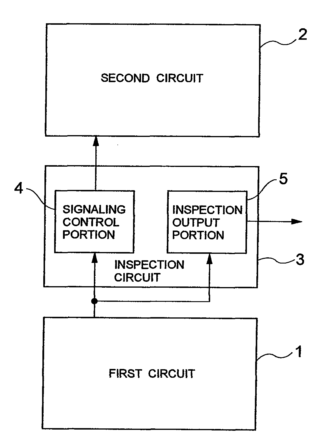
[0079]FIG. 1 is a schematic view illustrating a configuration of a first example of an inspection system according to the present invention. Referring to FIG. 1, the first example of the inspection system according to the present invention includes a first circuit 1, a second circuit 2 and an inspection circuit 3.

[0080]The inspection circuit 3 intervenes between the first circuit 1 and the second circuit 2. Further, the inspection circuit 3 includes a signaling control portion 4 and an inspection output portion 5. The signaling control portion 4 controls signaling between the first circuit 1 and the second circuit 2. Further, the inspection output portion 5 outputs an output of the first circuit 1 for inspection through the inspection circuit 3. According to the present invention, the signaling control portion 4 and the inspection output portion 5 share a part of the circuit to realize their own function with each other. Further, the first circuit 1, the second circuit 2 and the ins...

example 2

[0084]FIG. 3 is a schematic view illustrating a configuration of a second example of an inspection system according to the present invention. Referring to FIG. 3, the second example of the inspection system according to the present invention includes a first circuit 1, a second circuit 2 and an inspection circuit 3.

[0085]The inspection circuit 3 intervenes between the first circuit 1 and the second circuit 2. Further, the inspection circuit 3 includes a signaling control portion 4 and an inspection input portion 6. The signaling control portion 4 controls signaling between the first circuit 1 and the second circuit 2. Further, the inspection input portion 6 outputs an inspection signal to be input externally, to the second circuit 2 through the inspection circuit 3. In the present invention, the signaling control portion 4 and the inspection input portion 6 share a part of the circuit to realize their own function with each other. Further, the first circuit 1, the second circuit 2 a...

example 3

[0087]FIG. 4 is a schematic view illustrating a configuration of a third example of an inspection system according to the present invention. Referring to FIG. 4, the third example of the inspection system according to the present invention includes a first circuit 1, a second circuit 2 and an inspection circuit 3.

[0088]The inspection circuit 3 of the present invention intervenes between the first circuit 1 and the second circuit 2. Further, the inspection circuit 3 includes a signaling control portion 4, an inspection output portion 5 and an inspection input portion 6. The signaling control portion 4 controls signaling between the first circuit 1 and the second circuit 2. Further, the inspection output portion 5 outputs an output of the first circuit 1 for inspection through the inspection circuit 3. Further, the inspection input portion 6 outputs an inspection signal to be input externally, to the second circuit 2 through the inspection circuit 3. In the present invention, the sign...


PUM


Abstract

The present invention provides an inspection system with small increase in circuit area and capable of controlling increase in cost to be small. An inspection circuit intervenes between a first circuit and a second circuit. Further, the inspection circuit includes a signaling control portion and an inspection output portion. The signaling control portion controls signaling between the first circuit and the second circuit. Moreover, the inspection output portion outputs an output of the first circuit for inspection through the inspection circuit. In the present invention, the signaling control portion and the inspection output portion share a part of the circuit to realize their own function. Further, the first circuit, the second circuit and the inspection circuit are formed on the same substrate. The inspection circuit switches between the signaling control portion and the inspection output portion to use.

Description

BACKGROUND OF THE INVENTION[0001]1. Field of the Invention[0002]The present invention relates to an inspection system and an inspection circuit thereof, a semiconductor device, a display device, and a method of inspecting a semiconductor device, and more particularly, to an inspection circuit incorporated in a display device or a semiconductor device.[0003]2. Description of the Prior Art[0004]As technologies have been developed recently, a display device is made to fit for practical use, which incorporates, on a support substrate, various circuits such as a drive circuit which have been provided externally by using a LSI (Large Scale Integrated circuit) etc. conventionally formed by the silicon technology. An example of such a display device with a built-in circuit is a well-known display device formed by a high temperature polysilicon TFT (Thin Film Transistor) technology according to a high temperature process using an expensive quartz substrate. Further, a display device which ha...

Claims


Application Information

Patent Timeline
Patent Type & Authority Applications(United States)
IPC IPC(8): G01R31/26
CPCG01R31/319G09G3/006G01R31/31917
Inventor TAKATORI, KENICHI
Owner NEC CORP
Why Eureka
Try Eureka