3D electronic packaging structure having a conductive support substrate

a technology of conductive support and electronic packaging, which is applied in the direction of electrical equipment, semiconductor devices, semiconductor/solid-state device details, etc., can solve the problems of reducing yield and cost, reducing chip size, and reducing chip size, so as to reduce the manufacturing cost of each individual packaging unit, reduce the signal transmission path and time, and enhance the working frequency and efficiency of the stacked packaging module

Active Publication Date: 2007-12-27
ADVANCED CHIP ENG TECH
View PDF2 Cites 55 Cited by
  • Summary
  • Abstract
  • Description
  • Claims
  • Application Information

AI Technical Summary

Benefits of technology

[0007]The present invention proposes an electronic packaging structure, and the object is to provide a wafer-level packaging unit with multiple microelectronic elements, wherein the conductive trace patterns on the top and bottom surfaces can perform flexibly a single or multiple miniaturized stacked packaging structure depending on the requirements of application circumstances and functions to reduce the signal transmission paths and time, and thereby enhance the working frequency and efficiency of the stacked packaging module.
[0008]Another object of the invention is to provide an electronic packaging structure, wherein all packaging units are batch manufactured on the wafers or substrates, and thus reduce

Problems solved by technology

However, besides technical difficulties, integrating ever-complicated circuit functions into a single chip will enlarge the chip size, complicate the chip-making process, and causes reduced yield and increased cost.
The patent provides a wafer-level packaging structure having I/O fan-out characteristic; however, the packaging structure does not have stacking characteristic and

Method used


Image

  • 3D electronic packaging structure having a conductive support substrate
  • 3D electronic packaging structure having a conductive support substrate
  • 3D electronic packaging structure having a conductive support substrate

Examples


second embodiment

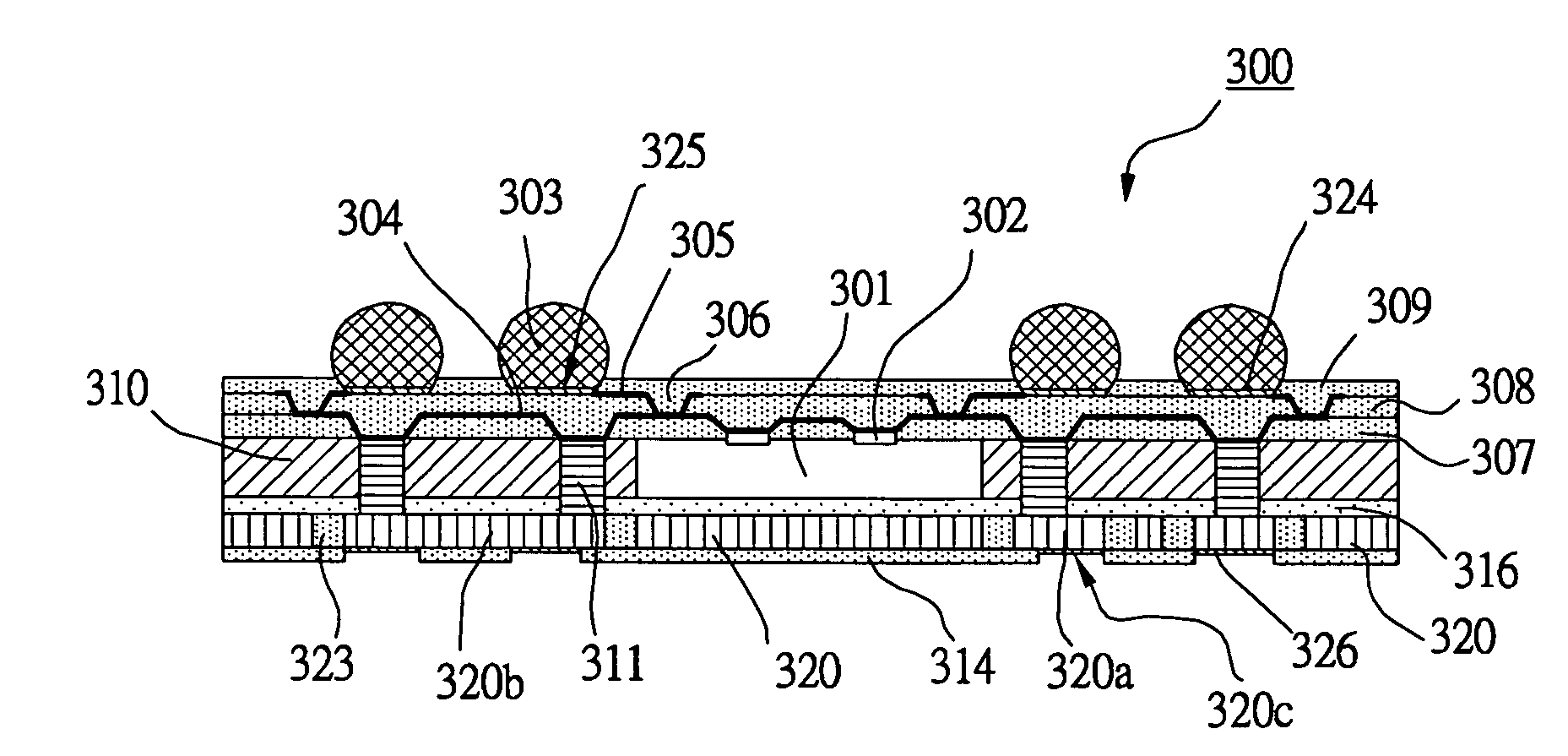
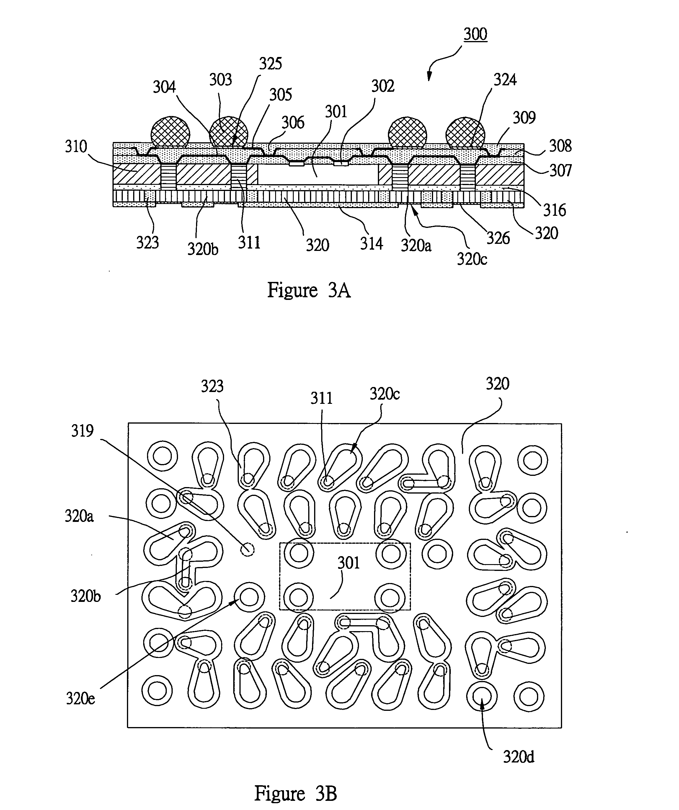
[0032]FIG. 4 is the present invention, and a cross-sectional schematic diagram of a first-type stacked packaging configured by the packaging units of the present invention. There are signal contacts on the corresponding spots of the top and bottom surfaces of a first packaging unit 410 and of a second packaging unit 420; signal transmission fixation structures 403 (UBM) can be utilized to form signal connection among the first packaging unit 410, the second packaging unit 420, and a substrate 401, and thereby completing a stacked packaging.

third embodiment

[0033]FIG. 5 is the present invention, and a cross-sectional schematic diagram of a second-type stacked packaging configured by the packaging units of the present invention. A first packaging unit 510, a second packaging unit 520, and a third packaging unit 530 can carry out stacking with a fourth packaging unit 540 of different size and all assembled on a substrate 501. The method of signal transmission between the packaging units can employ signal transmission fixation structures 503 (UBM), or signal transmission adhesive materials 505. Moreover, in order to enhance reliability of the whole packaging structure, adhesive materials 504 can be applied to the surrounding of signal transmission fixation structures 503 to enhance the strength of the fixation structures.

[0034]FIG. 6 is a fourth embodiment of the present invention, and a cross-sectional schematic diagram of a third-type stacked packaging configured by the packaging units of the present invention. A first packaging unit 61...

fifth embodiment

[0035]FIG. 7 is the present invention, and a cross-sectional schematic diagram of a fourth-type stacked packaging configured by the packaging units and unpackaged electronic elements of the invention. On a substrate 701, a first packaging unit 710 is connected thereon, and a second packaging unit 720 and a first electronic element 708 are carried on the first packaging unit 710. The electronic element 708 may be other forms of packaging units, or an unpackaged electronic element of any prior art. While stacking the packaging units, fixation structures of various sizes can be utilized to transmit circuit signals between the packaging units; as shown in the diagram, larger second signal transmission fixation structures 703 (UBM) are connected to first signal contacts 704, and smaller first signal transmission fixation structures 702 are connected to second signal contacts 705. Circuit signals can be transmitted between the second packaging unit 720 and the first electronic element 708...


PUM


Abstract

The present invention provides a 3D electronic packaging unit having a conductive supporting substrate that can achieve multi-chip stacking through the signal contacts on the both sides of the unit. The packaging unit can be batched manufactured on wafers or substrates, and thus reduce the manufacturing cost of each individual packaging unit; moreover, the conductive supporting substrate can be utilized to provide signal transmission of the electronic elements, and the supporting substrate can be used as a ground terminal for the carried electronic elements to enhance electric performance of the electronic elements. The supporting substrate is also a good thermal conductor that can release effectively heat energy generated by the electronic elements and accumulated inside the package to the outside of the package along the substrate to enhance reliability of the packaging structure.

Description

FIELD OF THE INVENTION[0001]The present invention relates to electronic packaging structures, and more particularly to a packaging unit having a conductive supporting substrate that can achieve multi-chip stacking through signal contacts on the both sides of the unit.BACKGROUND OF THE INVENTION[0002]As the demand for functions and applications of electronic products increases rapidly, packaging technology has continued to advance toward super high density, miniature, and from single chip to multi-chip, 2D to 3D scale. Consequently, there are advanced packaging structures (i.e. super high density packaging forms) at present, such as wafer level package, 3D package, multi-chip package, and System In Package (SIP), which are distinctly different from conventional packaging in the design, manufacture, and material use. The most ideal situation is to accommodate all circuits in a single silicon chip which is System-on-Chip (SoC). However, besides technical difficulties, integrating ever-...

Claims


Application Information

Patent Timeline
IPC IPC(8): H01L23/552
CPCH01L23/5389H01L2224/82102H01L24/24H01L25/105H01L2224/04105H01L2224/20H01L2224/24227H01L2224/76155H01L2924/01004H01L2924/01013H01L2924/01027H01L2924/01029H01L2924/01074H01L2924/01079H01L2924/15153H01L2924/1517H01L24/19H01L2224/0401H01L2224/32245H01L2924/07802H01L2924/01033H01L2924/01045H01L2924/01047H01L2224/16225H01L2224/12105H01L2224/32225H01L2224/73267H01L2225/1035H01L2225/1058H01L2225/1005H01L2924/10253H01L2924/00
Inventor YEW, MING-CHIHYUAN, CHANG-ANNCHOU, CHAN-YENCHIANG, KOU-NING
Owner ADVANCED CHIP ENG TECH
Why Eureka
Try Eureka