Methods for contact resistance reduction of advanced CMOS devices
- Summary
- Abstract
- Description
- Claims
- Application Information
AI Technical Summary
Benefits of technology
Problems solved by technology
Method used
Image

Examples
Embodiment Construction
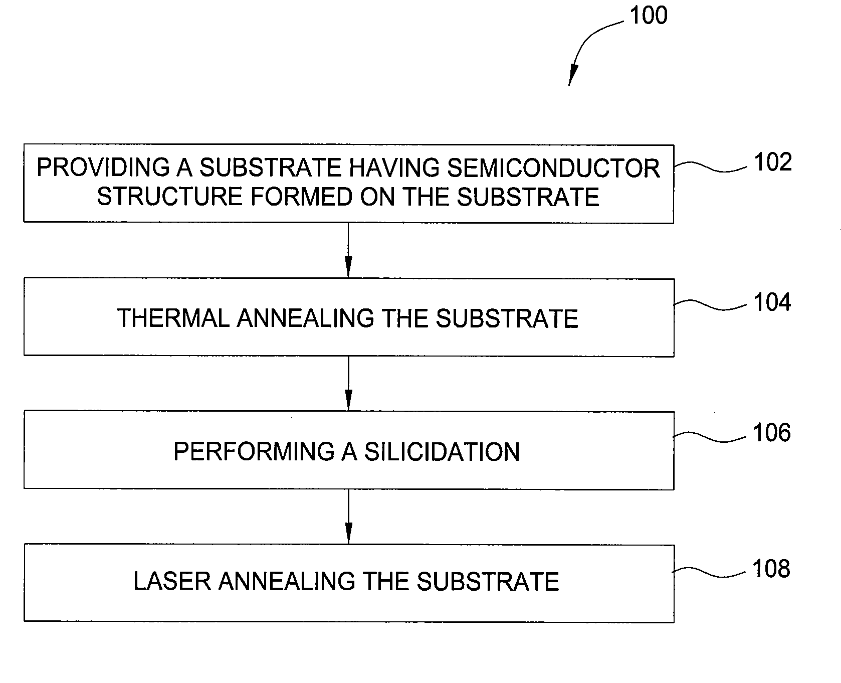
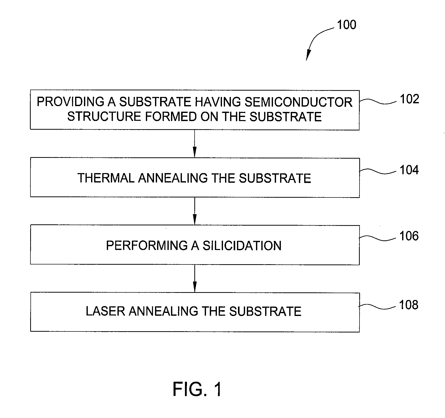
[0017]The present invention provides methods for reducing contact resistance in source / drain regions of semiconductor devices that have been thermally treated after dopant implantation. The contact resistance is reduced by a laser annealing process performed after a silicidation process. The laser annealing process performed after the silicidation process efficiently activates dopants accumulated on the interface of the silicon and silicide layer of source / drain junction during the silicidation process. The laser anneal activation process reactivates the dopants accumulated at the interface area of the silicon and silicide layer and redistributes dopants into lattice sites of the silicon layer that increases the overall dopant concentration in the source / drain regions after the silicidation process, thereby reducing contact resistance and improving device performance.
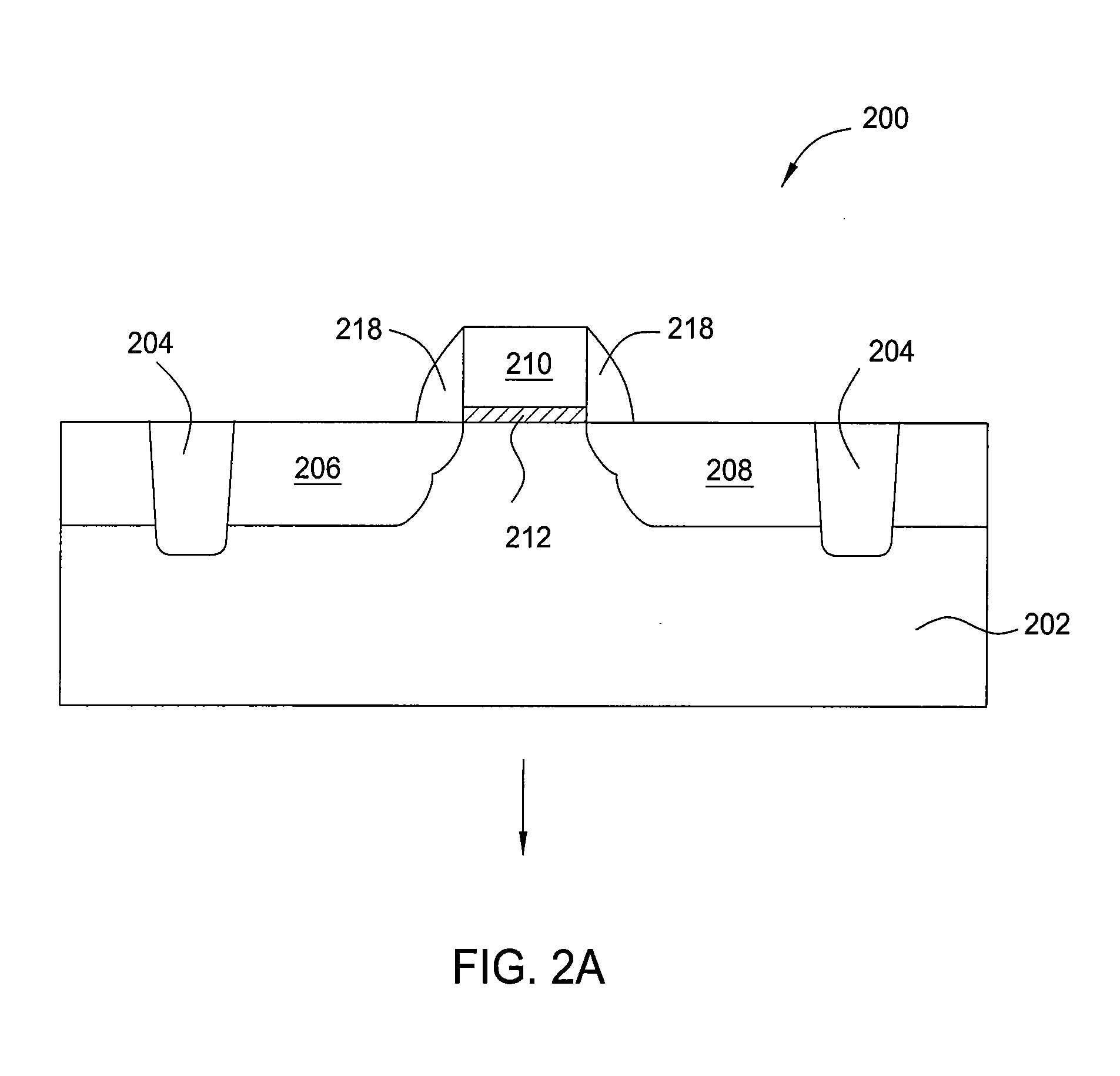
[0018]FIG. 1 illustrates a process flow diagram of one embodiment of a method 100 for laser annealing a substrate hav...
PUM
 Abstract
Description
Claims
Application Information
 - Generate Ideas
- Intellectual Property
- Life Sciences
- Materials
- Tech Scout
- Unparalleled Data Quality
- Higher Quality Content
- 60% Fewer Hallucinations
Browse by: Latest US Patents, China's latest patents, Technical Efficacy Thesaurus, Application Domain, Technology Topic, Popular Technical Reports.
© 2025 PatSnap. All rights reserved.Legal|Privacy policy|Modern Slavery Act Transparency Statement|Sitemap|About US| Contact US: help@patsnap.com