Method of forming isolation structure of semiconductor device for preventing excessive loss during recess gate formation

a technology of isolation structure and semiconductor device, which is applied in the direction of semiconductor devices, electrical devices, transistors, etc., can solve the problems of difficult crack filling when forming isolation structure for defining active regions, parasitic capacitance also increases, undesired loss a is caused in isolation structure, etc., to prevent excessive loss of isolation structure

Inactive Publication Date: 2008-01-03
SK HYNIX INC
View PDF3 Cites 25 Cited by
  • Summary
  • Abstract
  • Description
  • Claims
  • Application Information

AI Technical Summary

Benefits of technology

[0013]The embodiments of the present invention is directed to a method for forming an isolation structure of a semico

Problems solved by technology

As semiconductor devices become more highly integrated, trench filling when forming an isolation structure for defining an active region has become a difficult issue.
However, in the conventional art, when conducting the etching process for defining the groove for the formation of the recess gate, as shown in FIG. 2, an undesired loss A is caused in the isolation structure 140 (see FIGS. 1D and 2).
Further, if the loss A is caused in the isolation structure 140, the area of the isolation structure 14

Method used


Image

  • Method of forming isolation structure of semiconductor device for preventing excessive loss during recess gate formation
  • Method of forming isolation structure of semiconductor device for preventing excessive loss during recess gate formation
  • Method of forming isolation structure of semiconductor device for preventing excessive loss during recess gate formation

Examples


Embodiment Construction

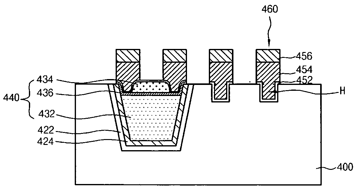
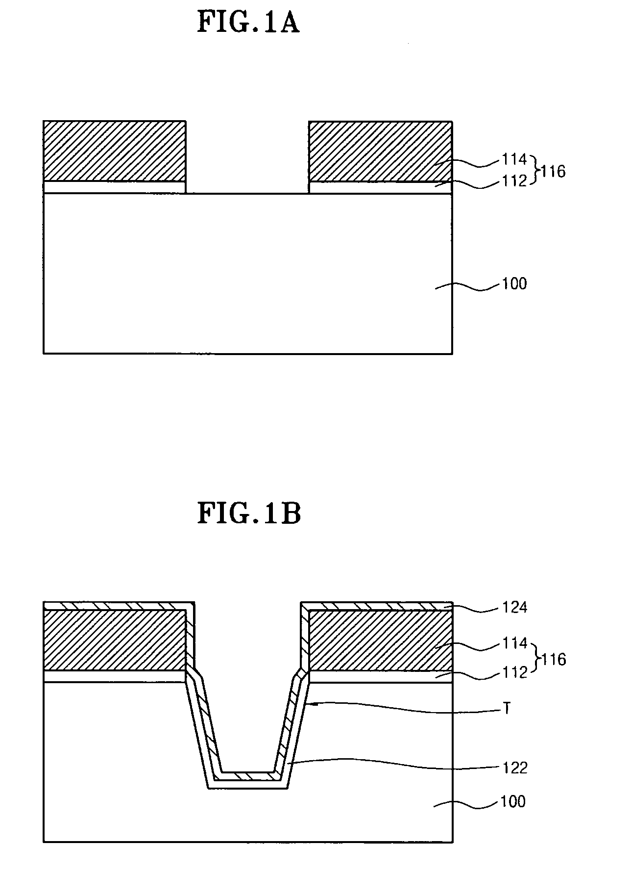
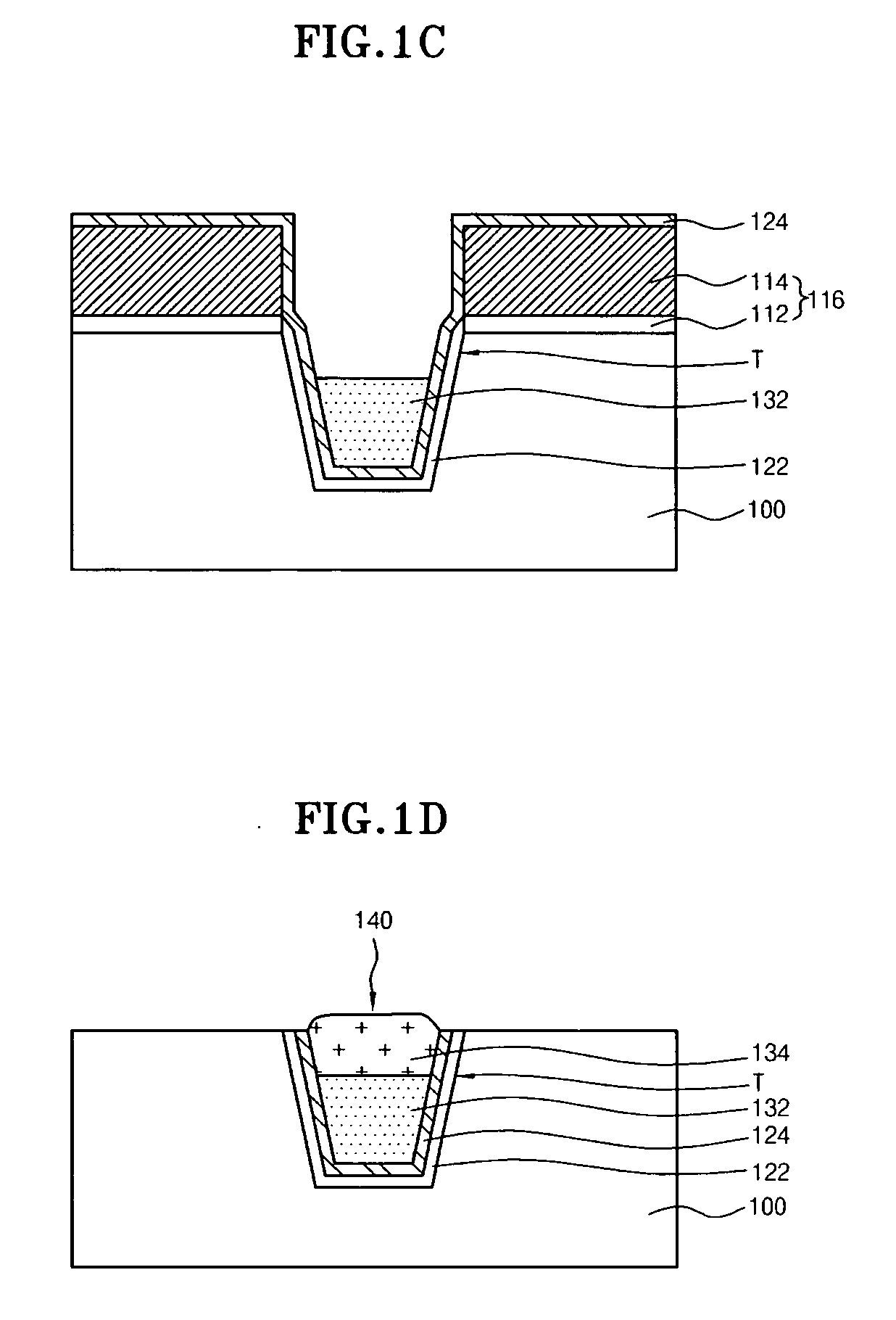
[0042]In an embodiment of the present invention, an SOG layer, a crystalline aluminum oxide (Al2O3) layer, and an HDP layer are sequentially filled in a trench, such that an isolation structure comprises a triple layer composed of these layers. In this case, because the crystalline aluminum oxide layer is not substantially lost even though it is exposed to a wet etching process or a cleaning process when forming a recess gate, the loss of the isolation structure can be minimized.

[0043]That is to say, in an embodiment of the present invention, because the isolation structure comprises the triple layer composed of the SOG layer, the aluminum oxide layer and the HDP layer, excessive loss of the isolation structure when forming a recess gate is prevented. Accordingly, the present invention prevents the occurrence of a short circuit between adjoining gates resulting from the excessive loss of the isolation structure. Also, in the present invention, because it is possible to prevent GIDL ...


PUM


Abstract

An isolation structure of a semiconductor device is formed by forming a hard mask layer on a semiconductor substrate having active and field regions to expose the field region. A trench is defined by etching the exposed field region of the semiconductor substrate using the hard mask as an etch mask. An SOG layer is formed in the trench partially filling the trench. An amorphous aluminum oxide layer is formed on the resultant substrate including the SOG layer. An HDP layer is formed on the amorphous aluminum oxide layer to completely fill the trench. The HDP layer and the amorphous aluminum oxide layer are subjected to CMP to expose the hard mask. The hard mask and portions of the amorphous aluminum oxide layer that are formed on the HDP layer are removed. The amorphous aluminum oxide layer is crystallized.

Description

CROSS-REFERENCE TO RELATED APPLICATIONS[0001]The present application claims priority to Korean patent application number 10˜2006˜0061369 filed on Jun. 30, 2006, which is incorporated by reference in its entirety.BACKGROUND OF THE INVENTION[0002]The present invention relates to a method for forming an isolation structure of a semiconductor device, and more particularly, to a method for forming an isolation structure of a semiconductor device that can prevent an excessive loss of an isolation structure when forming a recess gate.[0003]As semiconductor devices become more highly integrated, trench filling when forming an isolation structure for defining an active region has become a difficult issue. A method has been disclosed in the art for this situation in which a spin-on glass layer (hereinafter referred to as an “SOG layer”), with an excellent gap filling characteristic, is first deposited in the trench, and a high-density plasma-chemical vapor layer (hereinafter referred to as an...

Claims


Application Information

Patent Timeline
IPC IPC(8): H01L29/00
CPCH01L21/76224H01L21/76
Inventor SHEEN, DONG SUNSONG, SEOK PYOAHN, SANG TAEAN, HYEON JU
Owner SK HYNIX INC
Why Eureka
Try Eureka