Level conversion circuit

a level conversion and circuit technology, applied in logic circuits, pulse techniques, reliability increasing modifications, etc., can solve the problems of large imbalance between the rising edge delay of a signal affecting the operation at high rate, etc., to achieve sufficient setup time, reduce the difference between the rising edge delay and the falling edge delay, and achieve the effect of level conversion

Inactive Publication Date: 2008-01-03
ELPIDA MEMORY INC
View PDF6 Cites 13 Cited by
  • Summary
  • Abstract
  • Description
  • Claims
  • Application Information

AI Technical Summary

Benefits of technology

[0018]According to the present invention, it is possible to reduce the difference between the time necessary for the input signal to exceed a threshold of the first gate circuit when the input signal changes from the first logic level to the second logic level and the time necessary for the input signal to exceed the threshold of the first gate circuit when the input signal changes from the second logic level to the first logic level.
[0019]Accordingly, if the first power supply voltage is set lower than the amplitude of the input signal and the second power supply voltage and the first power supply voltage is supplied to a second gate circuit receiving the output from the first gate circuit, then level conversion can be performed between the input signal supplied to the first gate circuit and the output signal output from the second gate circuit, and the difference between the rising edge delay and the falling edge delay can be reduced.
[0020]As described above, according to the present invention, the difference between the rising edge delay of the signal and the falling edge delay thereof caused by the level conversion can be reduced. Therefore, it is possible to ensure a sufficient setup time and hold time of, for example, an address signal synchronous with a clock. It is thereby possible to ensure that a semiconductor device using the level conversion circuit according to the aspect of the present invention operates at high rate.

Problems solved by technology

In this way, if the conventional level conversion circuit is employed, a large imbalance is produced between the rising edge delay of a signal and a falling edge delay thereof due to the level conversion.
This disadvantageously hinders operation at high rate.

Method used


Image

  • Level conversion circuit
  • Level conversion circuit
  • Level conversion circuit

Examples


Embodiment Construction

[0026]Preferred embodiment of the present invention will now be explained in detail with reference to the drawings.

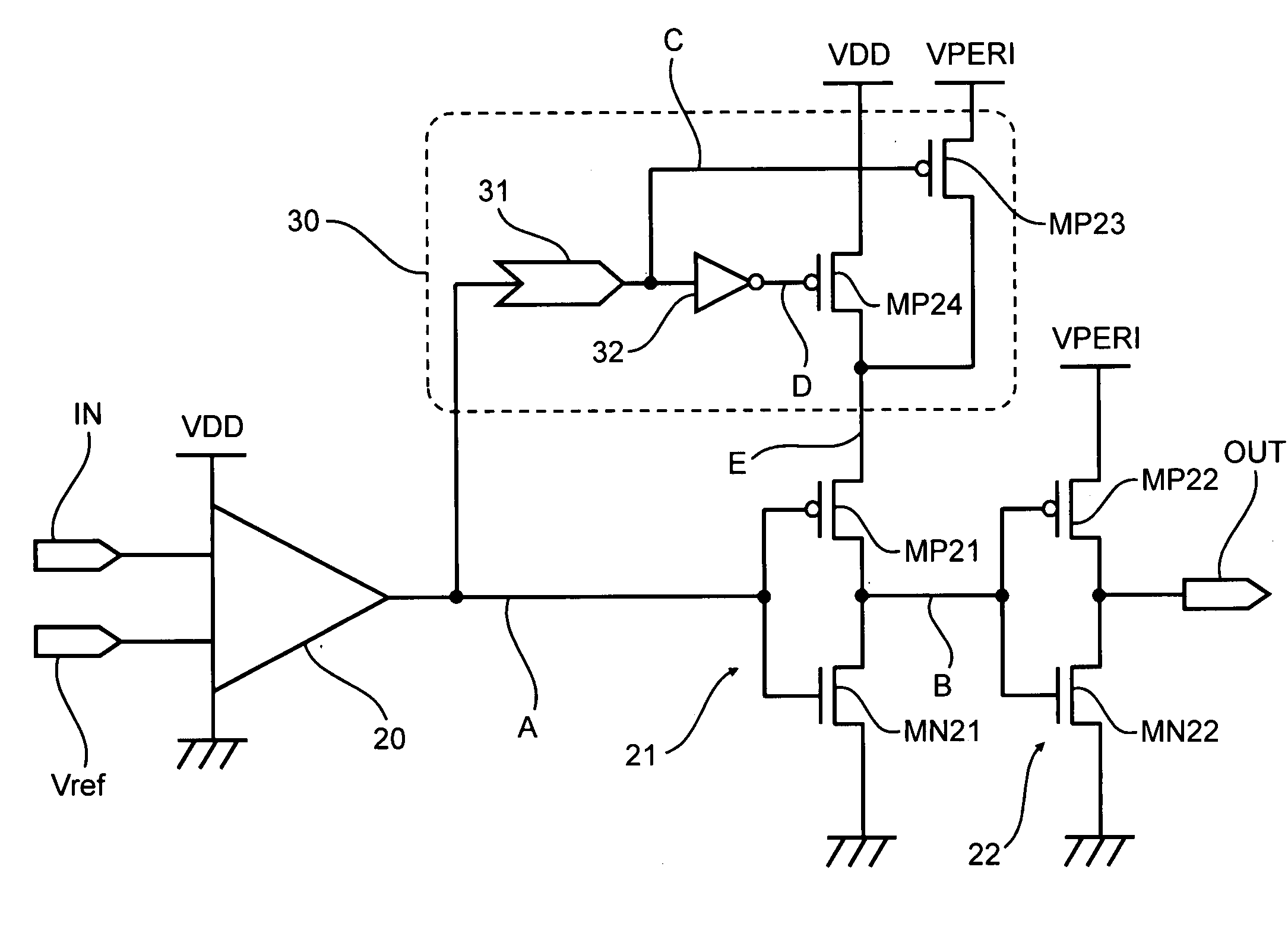
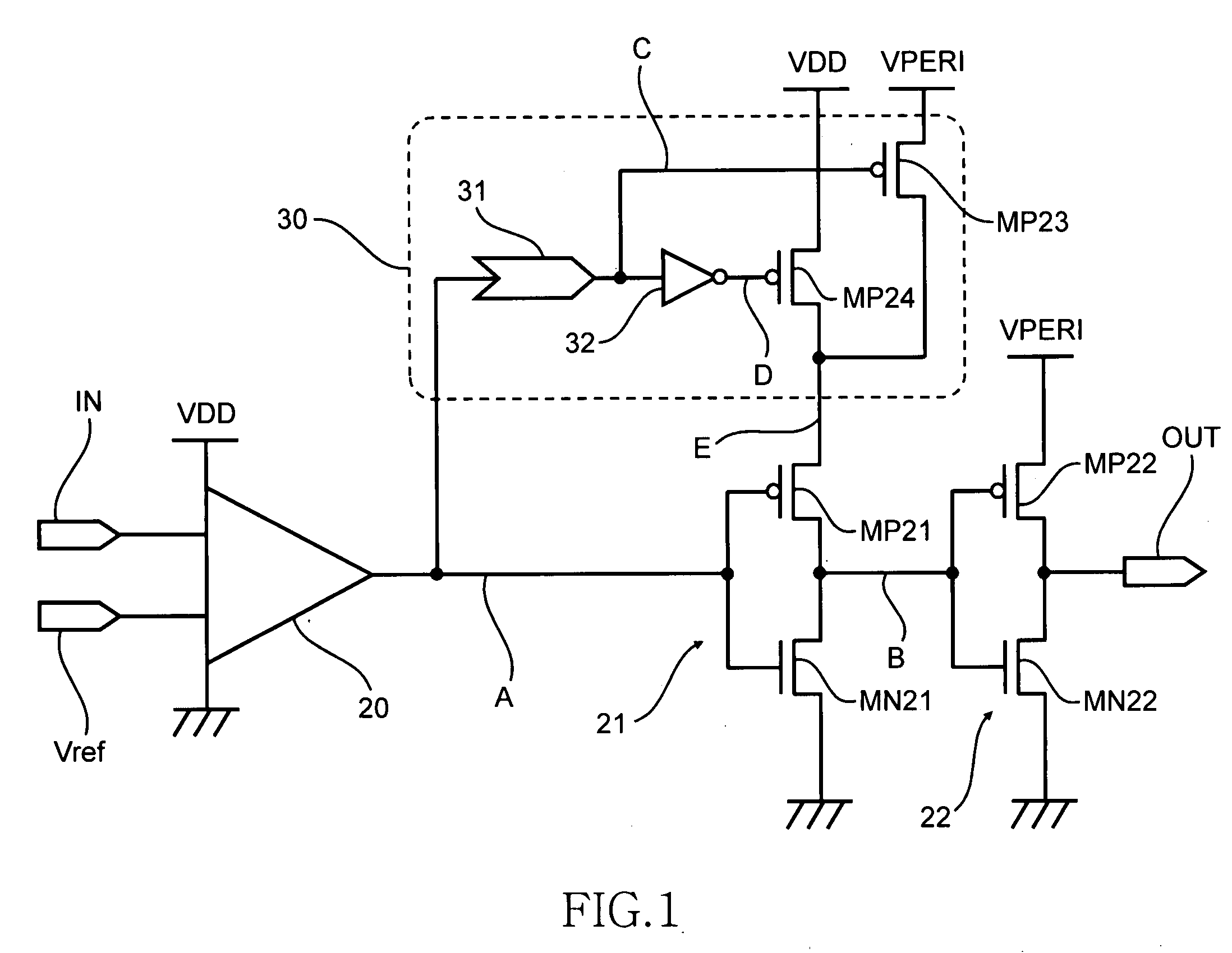
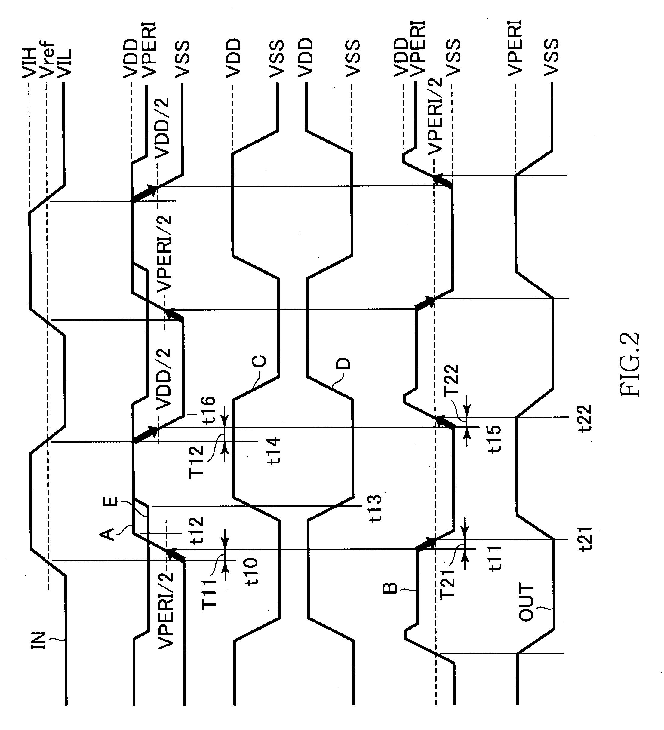
[0027]FIG. 1 is a circuit diagram of a level conversion circuit according to a preferred embodiment of the present invention.

[0028]As shown in FIG. 1, the level conversion circuit according to the present embodiment includes an input buffer 20 receiving an external signal and inverter circuits 21 and 22 arranged in rear of the input buffer 20 and cascade-connected to each other. The level conversion circuit shown in FIG. 1 is similar in a basic configuration of to ordinary level conversion circuits.

[0029]The input buffer 20 is a buffer that receives a signal in the form of, for example, SSTL (Stab Series Terminated Logic). An external signal IN is supplied to one of input terminals of the input buffer 20 whereas a reference voltage Vref is supplied to the other input terminal of the input buffer 20. By so configuring the input buffer 20, a signal A output from the input...


PUM


Abstract

A level conversion circuit includes an input buffer receiving an external signal, cascade-connected inverter circuits arranged in rear of the input buffer, and a switching circuit supplying an internal power supply potential to a power supply terminal of the inverter circuit while an input signal input to the inverter circuit changes from low level to high level, and supplying an external power supply potential to the power supply terminal while the input signal changes from the high level to the low level. The difference between a time necessary for the input signal to exceed a threshold of one of the inverter circuits when the input signal changes from the low level to the high level and time necessary for the input signal to exceed the threshold of the inverter circuit when the input signal changes from the high level to the low level can be thereby reduced.

Description

TECHNICAL FIELD[0001]The present invention generally relates to a level conversion circuit for converting amplitude of an electric signal, and particularly relates to a level conversion circuit capable of reducing the difference between a rising edge delay of a signal and a falling edge delay thereof due to level conversion.BACKGROUND OF THE INVENTION[0002]In recent years, many techniques for reducing an operating voltage of a semiconductor device have been proposed and put to practical use mainly for purposes of reduction of power consumption. There are known some semiconductor devices based on a technique for setting an external voltage to a high voltage similarly to a conventional method and for using a reduced voltage from the high voltage as an internal voltage to ensure compatibility with an existing semiconductor device. In case of a semiconductor device based on such a technique, the amplitude of an external signal or a signal output from an input buffer, to which the extern...

Claims


Application Information

Patent Timeline
Patent Type & Authority Applications(United States)
IPC IPC(8): H03K19/0175
CPCH03K19/018521H03K19/00323
Inventor NAGATA, KYOICHI
Owner ELPIDA MEMORY INC
Why Eureka
Try Eureka